Liquid crystal display having an opening in each pixel electrode corresponding to each storage line

Inactive Publication Date: 2003-06-24
PANASONIC LIQUID CRYSTAL DISPLAY CO LTD +1
View PDF5 Cites 20 Cited by
  • Summary
  • Abstract
  • Description
  • Claims
  • Application Information

AI Technical Summary

Benefits of technology

It is an object of the present invention to provide a liquid crystal display element capable of suppressing occurrence of flicker and brightness grading in a display by solving the problems with the prior art, facilitating the establishment of a desired storage capacitance, and reducing a storage capacitance, wiring capacitances formed by gate lines or drain lines, and further capable of improving a manufacturing tact.
To achieve the above object, the present invention is capable of establishing the storage capacitance value in accordance with the storage line by providing an opening in a pixel electrode, reducing wiring capacitances of gate lines and / or drain lines by providing cutouts in a portion of a common electrode overlying (or being located at an opposite side of the liquid crystal layer to) the gate lines and / or the drain lines (e.g. by eliminating the portion of the common electrode so as to form an opening therein), or supplying a voltage to the common electrode or the storage lines by providing column-like conductive spacers between the common electrode and the storage lines without a conductive paste.

Problems solved by technology

The storage capacitance Cstg is determined by the area of the overlap between the pixel electrode ITO1 and the storage line STL, and is therefore determined by the shape and dimensions of the storage line, and consequently, the exact establishment of the storage capacitance Cstg is difficult, and also the resistance is increased.
The common electrode ITO2 also overlies the gate lines GL and the drain lines DL with the liquid crystal layer interposed therebetween, and therefore a large wiring capacitance is formed between the common electrode ITO2 and the drain and gate lines GL, DL, and consequently delay caused by wiring produces brightness grading in a display image.
Consequently, there is a problem in that flicker or brightness grading occurs in a displayed image.
However, there is a problem in that, the longer the storage lines, the larger the resistance and a wiring capacitance, and fluctuations in potentials occur, and consequently, flicker and brightness grading occur in a display and they deteriorate the quality of the display.
In a driving method employing the common-electrode voltage inversion, it is difficult to reduce the number of the points for voltage supply because a signal is supplied to the common electrode.

Method used


Image

  • Liquid crystal display having an opening in each pixel electrode corresponding to each storage line
  • Liquid crystal display having an opening in each pixel electrode corresponding to each storage line
  • Liquid crystal display having an opening in each pixel electrode corresponding to each storage line

Examples


third embodiment

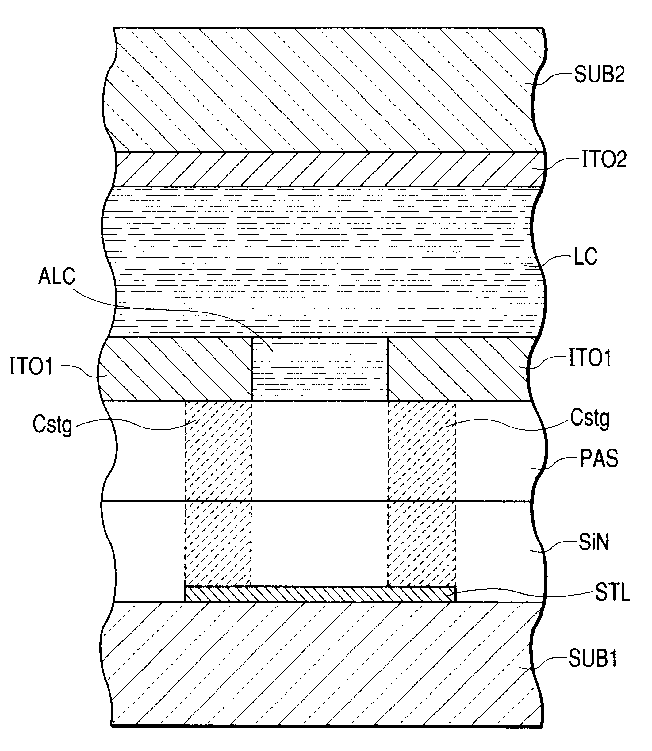
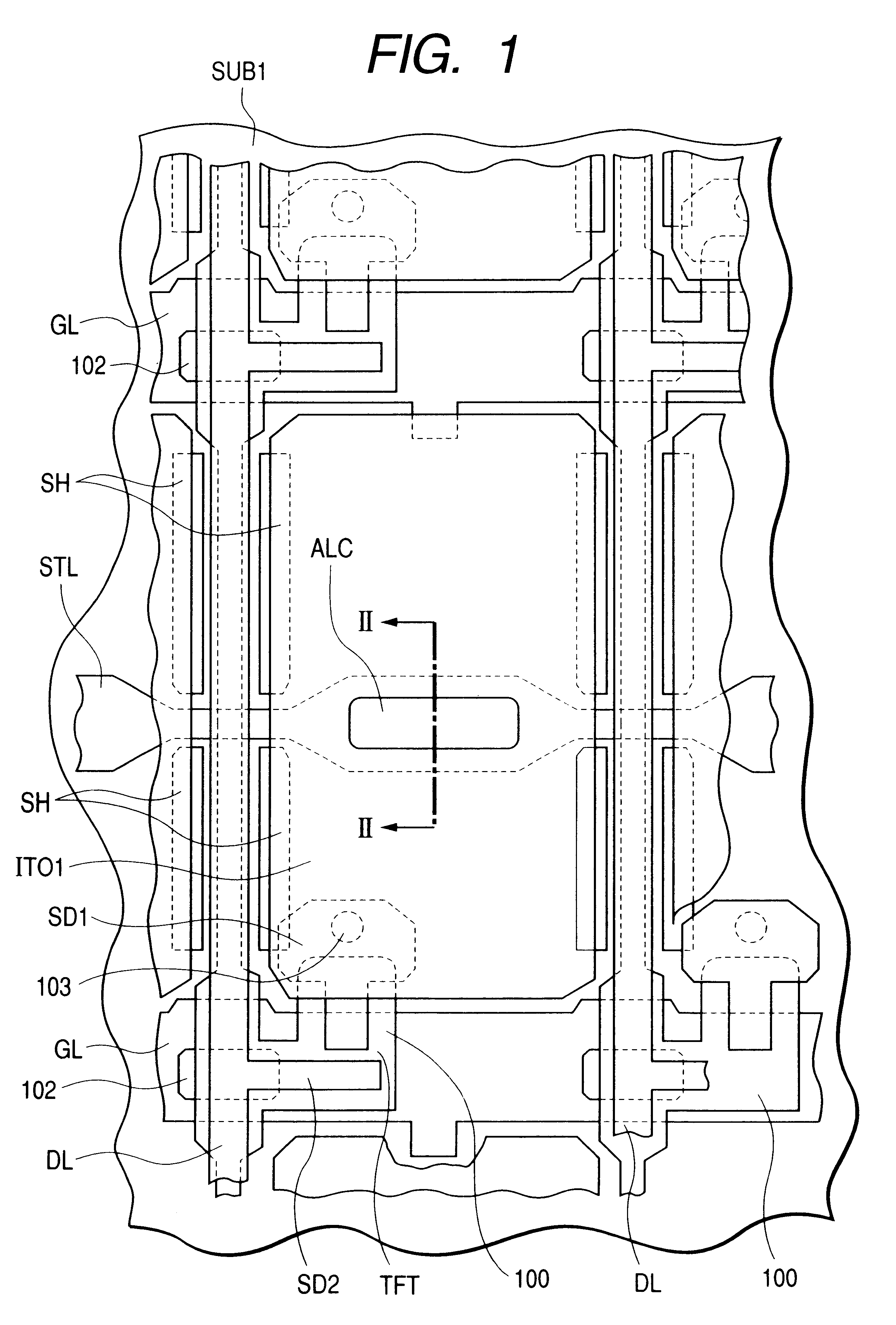
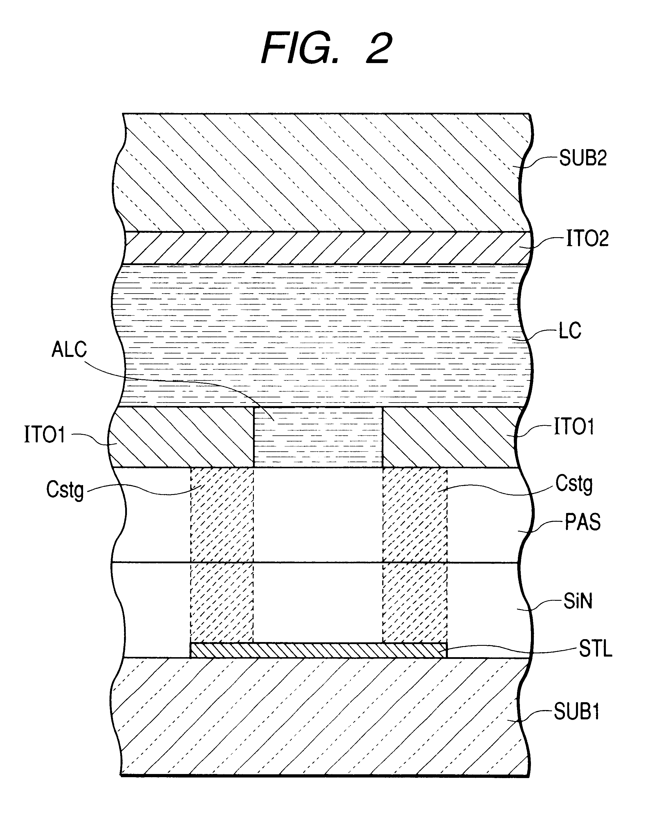
FIG. 5 is a plan view of essential parts of the liquid crystal display element of the present invention for explaining a configuration of its storage line STL portion, and FIG. 6 is a schematic cross-sectional view of the liquid crystal display element taken along line VI--VI of FIG. 5. In FIGS. 5 and 6, reference character SOC denotes a conductive column-like spacer, SH is a light-shielding member, and the same reference characters and numerals as utilized in FIGS. 1-4 designate functionally corresponding portions in FIGS. 5 and 6.

The conductive column-like spacer SOC is shaped from a photosensitive resin having carbon black dispersed therein or a conductive polymer, for example. For the former, a material capable of being hardened by photolithography is suitable for the photosensitive resin. For the latter, for example, the conductive polymer may be a material belonging to poly-acetylene system, poly-phenylene system, etc. mixed with dopants such as an arsenic compound AsF.sub.5, ...

fourth embodiment

FIG. 7 is a plan view of essential parts of the liquid crystal display element of the present invention for explaining a configuration of its storage line STL portion, and FIG. 8 is a schematic cross-sectional view of the liquid crystal display element taken along line VIII--VIII of FIG. 7. In FIGS. 7 and 8, reference character ITO3 denotes a conductive layer, and the same reference characters and numerals as utilized in FIGS. 1-6 designate functionally corresponding portions in FIGS. 7 and 8.

embodiment 3

In this embodiment, the conductive layer ITO3 is formed to cover the storage line STL at the bottom of the opening ALCN in Embodiment 3, and the conductive column-like spacer SOC is formed on the conductive layer ITO3.

The configuration of this embodiment prevents corrosion of the otherwise storage line STL, and thereby provides stable display characteristics for a long period of time in addition to the advantage provided by Embodiment 3.


PUM


Abstract

A liquid crystal display element includes a pair of substrates, a liquid crystal layer sandwiched therebetween, gate lines and drain lines disposed to intersect the gate lines disposed on one of the substrates, thin film transistors disposed at the intersections of the gate and drain lines, pixel electrodes disposed in an area surrounded by two adjacent gate lines and two adjacent drain lines, a common electrode disposed on the other substrate. The liquid crystal display element is also provided with storage lines disposed below the pixel electrodes with an insulating layer interposed therebetween to form a capacitance therebetween. Each of the pixel electrodes is formed with an opening in a portion thereof facing the storage lines.

Description

BACKGROUND OF THE INVENTIONThe present invention relates to a liquid crystal display element, and in particular to a thin film transistor active-matrix type liquid crystal display element provided with a storage capacity formed in a pixel area by a storage line disposed therein and a pixel electrode.Liquid crystal display devices are widely used as a high-definition color display device for a notebook computer and a display monitor.Among liquid crystal display elements, the simple matrix type and the active matrix type are well-known. The simple matrix type liquid crystal display element comprises a pair of opposing substrates, a first group of parallel strip electrodes disposed on an inner surface of one of the substrates, a second group of parallel strip electrodes disposed on an inner surface of the other substrate to intersect the first group of parallel strip electrodes, and a liquid crystal layer sandwiched between the substrates. The active matrix type liquid crystal display ...

Claims


Application Information

Patent Timeline
IPC IPC(8): G02F1/13G02F1/1362G02F1/1343
CPCG02F1/136213G02F1/134336G02F2201/123G02F1/1343
Inventor OOTSU, RYOUICHIOHGIICHI, KIMITOSHI
Owner PANASONIC LIQUID CRYSTAL DISPLAY CO LTD
Why Eureka
Try Eureka