Pixel structure, array substrate and display device

A pixel structure and pixel electrode technology, applied in nonlinear optics, instruments, optics, etc., can solve the problems of reducing aperture ratio, high load of scanning lines, rising cost of backlight module, etc., to achieve reduced storage capacitance, high transparency excessive effect

Inactive Publication Date: 2016-07-06
BOE TECH GRP CO LTD
View PDF6 Cites 0 Cited by
  • Summary
  • Abstract
  • Description
  • Claims
  • Application Information

AI Technical Summary

Problems solved by technology

In order to further improve product quality, especially the imaging quality of dynamic images, high-frequency drive display devices are favored by more manufacturers. Due to the large storage capacitance (storage capacitance) in the pixel structure of advanced ultra-dimensional field switching display devices, When it is driven at high frequency, its scanning line needs a higher load, so the width of the scanning line needs to be increased, but this will inevitably reduce the aperture ratio, which will lead to an increase in the cost of the backlight module

Method used


Image

  • Pixel structure, array substrate and display device
  • Pixel structure, array substrate and display device

Examples


Embodiment Construction

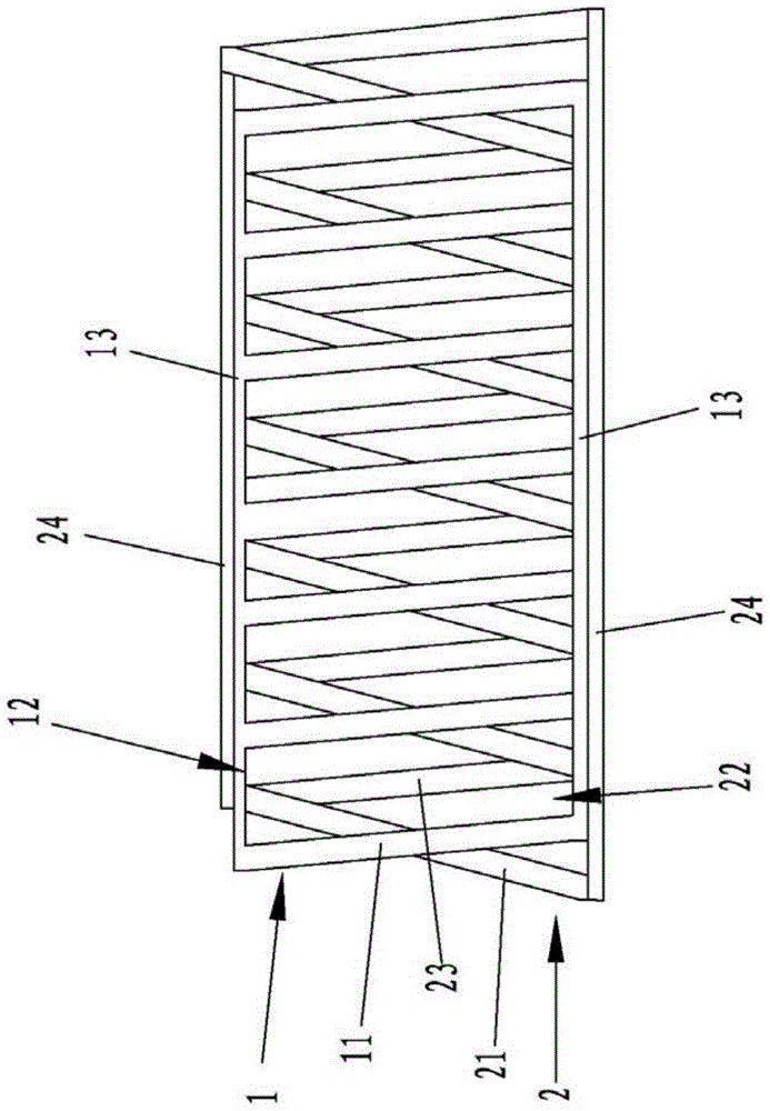
[0020] The technical solution of the present invention is to reduce the storage capacitance, and the second electrode is designed with slit patterning. This design maintains a high transmittance and process yield on the basis of reducing the storage capacitance.

[0021] Such as figure 1 As shown, the embodiment of the pixel structure of the present invention includes a first electrode 1 and a second electrode 2 located below the first electrode 1, the first electrode 1 and the second electrode 2 are not conductive, and the first electrode 1 includes A plurality of strip-shaped first electrode parts 11 arranged in parallel and equidistant and a plurality of first gaps 12 between adjacent first electrode parts 11, the second electrode 2 includes a plurality of strip-shaped and parallel and equidistantly arranged The second electrode part 21 and a plurality of second gaps 22 between the adjacent second electrode parts 21, the downward vertical projection of each first electrode ...


PUM


Abstract

The invention discloses a pixel structure, an array substrate and a display device. The pixel structure comprises a first electrode and a second electrode, wherein the first electrode comprises a plurality of first electrode parts and a plurality of first gaps located between the adjacent first electrode parts, the second electrode comprises a plurality of parallel strip-shaped second electrode parts and a plurality of second gaps located between the adjacent second electrode parts, the downward perpendicular projection of each first electrode part is overlapped with the downward perpendicular projection of each second electrode part, the second electrode comprises third electrode parts, and each second electrode part is connected with the adjacent electrode part through one third electrode part. The array substrate comprises the pixel structure. The display device comprises the array substrate. According to the technical scheme, storage capacitance is reduced, the second electrode is designed in a narrow gap patterning mode, and on the basis of reducing the storage capacitance, high transmittance and high technological yield are maintained.

Description

technical field [0001] The invention belongs to the technical field of liquid crystal display, and in particular relates to a pixel structure, an array substrate and a display device. Background technique [0002] With the development of thin film field effect transistor liquid crystal display (ThinFilmTransistorLiquidCrystalDisplay, TFT-LCD) technology and the advancement of industrial technology, the production cost of liquid crystal display devices has been reduced, and the manufacturing process has become increasingly perfect. TFT-LCD has replaced the cathode ray tube display as a flat panel display mainstream technology in the field. [0003] Due to the improvement of living standards, customers' requirements for display devices have also been further improved. Display devices with high refresh rate and high display quality have become the mainstream. At the same time, in order to strengthen product competitiveness, reducing the cost of display devices has become an ine...

Claims


Application Information

Patent Timeline
Patent Type & Authority Patents(China)
IPC IPC(8): G02F1/1343G02F1/1368
Inventor 王强涛林允植崔贤植严允晟
Owner BOE TECH GRP CO LTD
Why Eureka
Try Eureka