
Clock distribution network planning and method therefor

a technology of distribution network and clock, applied in the direction of generating/distributing signals, instruments, program control, etc., can solve the problems of data as a whole improperly propagating down the chain, etc., to reduce the adverse effects of clock skew

Inactive Publication Date: 2001-10-16
BELL SEMICON LLC
View PDF15 Cites 87 Cited by
  • Summary
  • Abstract
  • Description
  • Claims
  • Application Information

AI Technical Summary

Benefits of technology

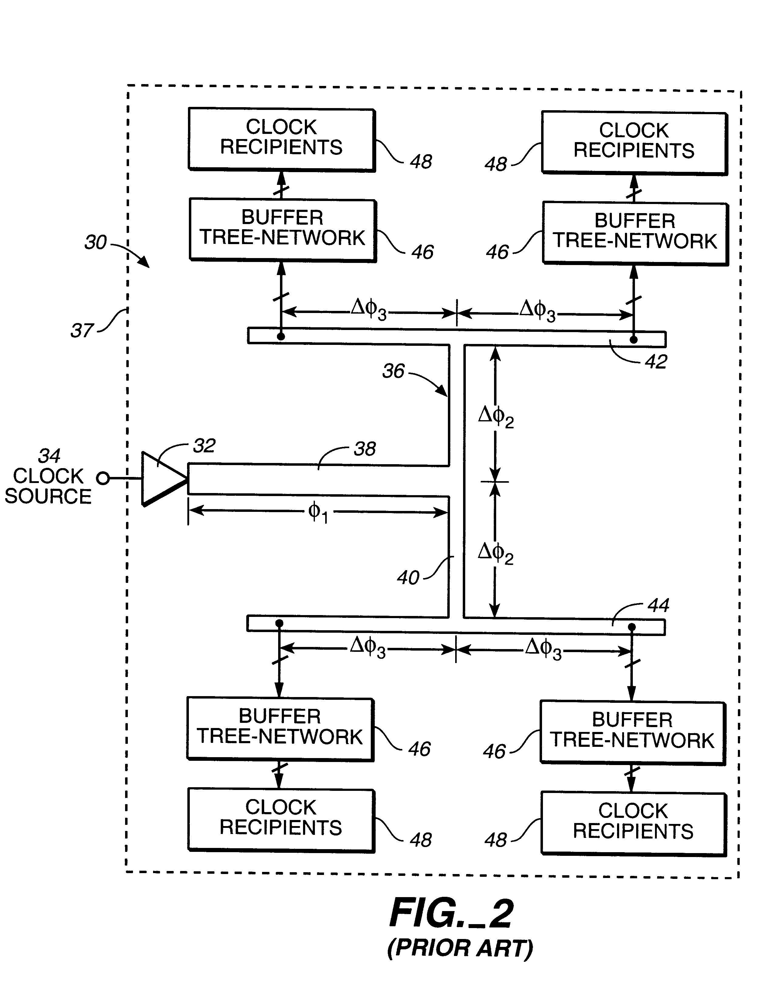
, the balanced clock tree 30 routes the clock signal in an ASIC in a manner that the phases of the clock signals at the clock inputs of the clock recipients are substantially the same. This is done by providing an H-tree conductive structure 36 for providing the initial distribution of the clock signal from the ASIC clock input to the inputs of the buffer tree-networks 46 in a manner that the phases of the clock signal thereat are substantially the same. The buffer tree-network 46 includes clock routing networks (e.g., 50 and 54) for providing the clock signal to the buffers in a manner that the phases of the clock signal at the output of each of the buffer within one level are substantially the same. Another similar clock routing network is provided at the output of the last level of buffers so that the clock signal is provided to the clock input of the clock recipients in a manner that the phases of the clock signal thereat are substantially the same. This type of clock distribution reduces the adverse effects of clock skew.
Therefore, there is a need for methods and computer-aided design tools for planning the clock distribution network in the conceptual design phase of the ASIC devices to reduce clock skew, ground bounce, VDD noise and idle clock cycle time, and avoid the difficulty of balancing the clock distribution network in the latter stages of the ASIC design.
FIG. 2 is a schematic and block diagram of a prior art balanced clock tree used for reducing the effects of clock skew.
FIG. 3 is a schematic and block diagram of a prior art buffer network or tree as an element of the prior art balanced clock tree of FIG. 2, wherein the buffer network or tree distributes the clock signal to clock recipient elements in a manner that it reduces clock skew.

Problems solved by technology

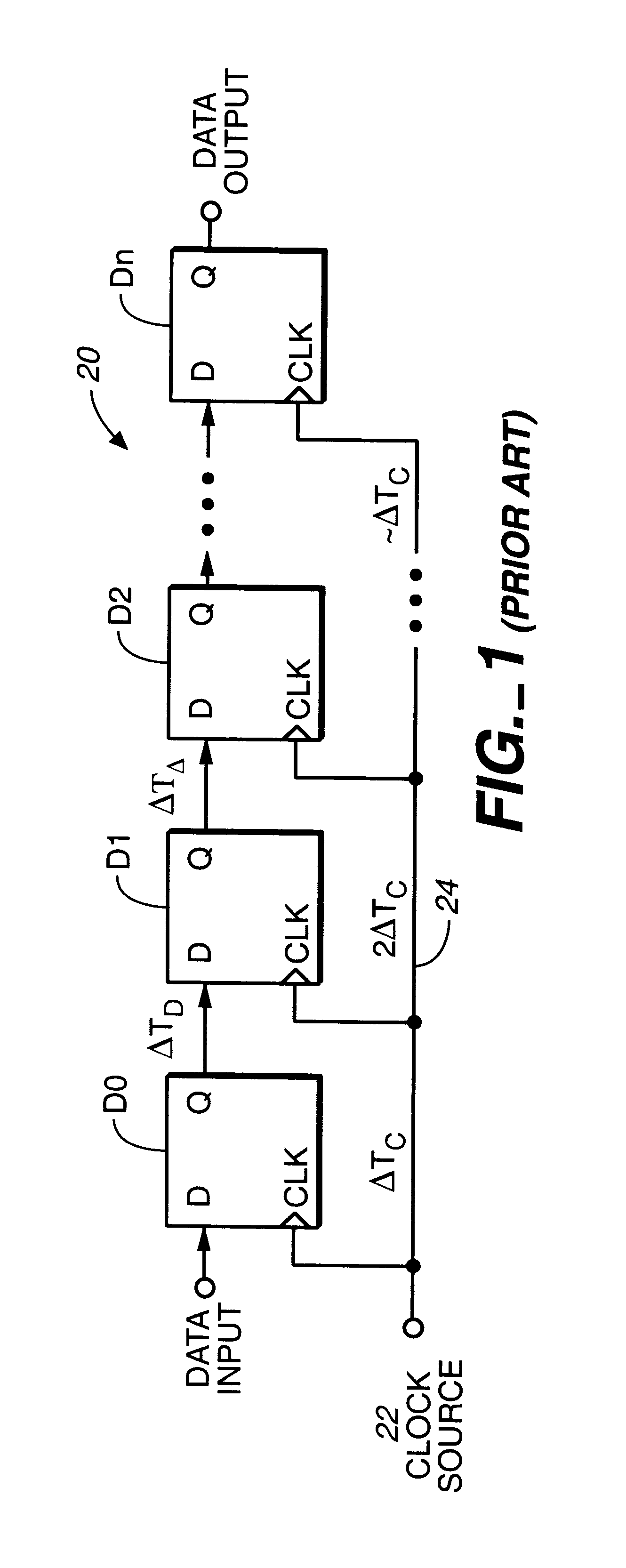
This results in the data not properly propagating as a whole through the chain; a condition generally termed in the art as "clock skew."
However, with the clock distribution network 24 shown in FIG. 1, problems occur for flip-flops down the chain 20.
This results in the data as a whole improperly propagating down the chain 20.
Sometimes, however, it may be difficult because of layout reasons to provide a conductive line of a sufficient length to equalize the clock signal phases at the inputs of the buffers.
Although the balanced clock tree 30 is useful for reducing clock skew problems, there may be disadvantage to it when the number of clock recipients in an ASIC becomes large.
One disadvantage of the balanced clock tree is that when the number of clock recipient becomes large, problems such as ground bounce and V.sub.DD noise results.
The result is that it takes a relatively large current to clock all those clock recipients at substantially the same time.
The same large current during clocking also results in the V.sub.DD voltage supply to drop during clocking of the clock recipients, which causes noise on the V.sub.DD line.
Another disadvantage is that it becomes increasingly difficult to layout or balance the clock distribution network when the number of clock recipient becomes large.
Many ASIC design ECAD systems perform the layout and the balancing of the clock distribution network during the physical design stage of design, which may prove to be too late for effective balancing of the clock distribution network when the number of clock recipient becomes very large.
Furthermore, another disadvantage of the prior art clock distribution network and the design method is the possibility of unused cycle time.

Method used


Image

  • Clock distribution network planning and method therefor
  • Clock distribution network planning and method therefor
  • Clock distribution network planning and method therefor

Examples


Embodiment Construction

FIG. 6 illustrates a flow diagram for providing an overview of ASIC chip design according to preferred embodiments of the present invention. It should be understood that the description contained herein are in terms of a suite of software "blocks" that can be run on any suitable computer system.

In step 100, an IC system design specification is prepared. The preparation in step 100 consists of system or device specification and may include functional specifications of subsystem elements, timing specifications and I / O requirements, and power, package and interface requirements. At this initial step of the design cycle, the desired system design is described in the highest level of abstraction.

In step 110, a technology-independent description is produced by formulating a behavioral description of the circuit's desired behavior in a high-level hardware description language (HDL), such as VHDL or Verilog-HDL. Instead of being formulated in a behavioral description, the technology-indepen...


PUM


Abstract

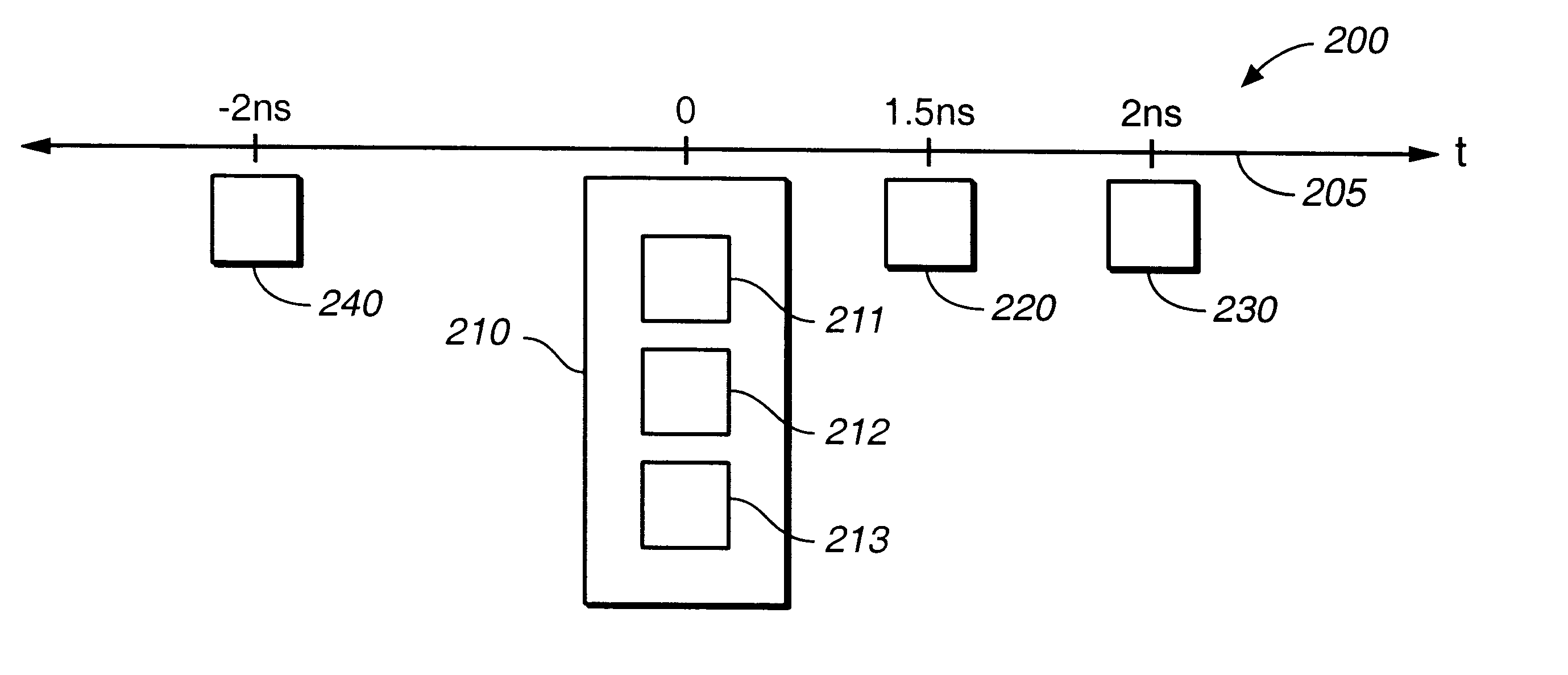
A method for planning the clock distribution network in the conceptual design phase of an ASIC device is provided herein that comprises partitioning the technology-independent description of the device into partitioned groups based on the clocking time of the clock recipients in each of the partitioned groups. In addition, a clock budgeting plan is generated by creating target timing groups and assigning each of the partitioned groups to one of the target timing groups based on the clocking time of the clock recipients in each of the partitioned groups. The clock recipients in each of the target timing groups clock at a substantially same time and clock recipients in different target groups clock at different times. The clock distribution network is created based on the clock budgeting plan such that the clock distribution network provides a clock signal to clock recipients in each of the target timing groups in a manner that the clock recipients in each of the target timing groups are clocked together at a substantially same time.

Description

1. Field of the InventionThis invention relates generally to clock distribution network planning for ASICs, and in particular, to methods and computer-aided design tools for planning the clock distribution network in the conceptual design phase of the ASIC devices to reduce clock skew, ground bounce, VDD noise and idle clock cycle time.2. Description of the Related ArtThe routing and distribution of the clock to elements of an integrated circuit, or more specifically, an application specific integrated circuit (ASIC), is an important factor to consider in the design of ASICs. To take an analogy, for instance, the clock of an ASIC may be seen as the heart and blood flow of a human body, whereas the clock routing and distribution of an ASIC may be seen as the arteries and veins of a human body. Just like the human body requires that the arteries and veins be properly distributed in order for each organ to function properly and together with other organs, the clock routing and distribu...

Claims


Application Information

Patent Timeline
IPC IPC(8): G06F17/50G06F1/10
CPCG06F1/10G06F17/5045G06F30/30
Inventor GRAEF, STEFAN
Owner BELL SEMICON LLC
Learn More