Planar stitched write head having write coil insulated with inorganic insulation
- Summary
- Abstract
- Description
- Claims
- Application Information
AI Technical Summary
Benefits of technology
Problems solved by technology
Method used
Image
Examples
second embodiment
OF THE PRESENT INVENTION
FIGS. 11 and 12 show a second embodiment 250 of the present write head. The write head 250 includes a first pole piece 252 which is planar from the ABS to and past the back gap (BG). The write gap layer 254 is located on the first pole piece 252 from the ABS to at least the back gap (BG). The write gap layer 254 serves as an etch step in this embodiment, which will be described in detail under the method of construction of the second embodiment. A second pole tip layer 256 is located on the write gap layer 254 in the pole tip region and a write coil layer 258 is located on the write gap layer 254 in the yoke region. A write coil insulation layer 260 is located between the turns of the write coil 258 and between the write coil and the second pole tip layer 256. Top surfaces of the second pole tip 256, the write coil layer 258, and the write coil insulation layer 260 form a common flat surface. The top insulation layer 262 is located on the top flat surface and...
first embodiment
METHOD OF MAKING FIRST EMBODIMENT
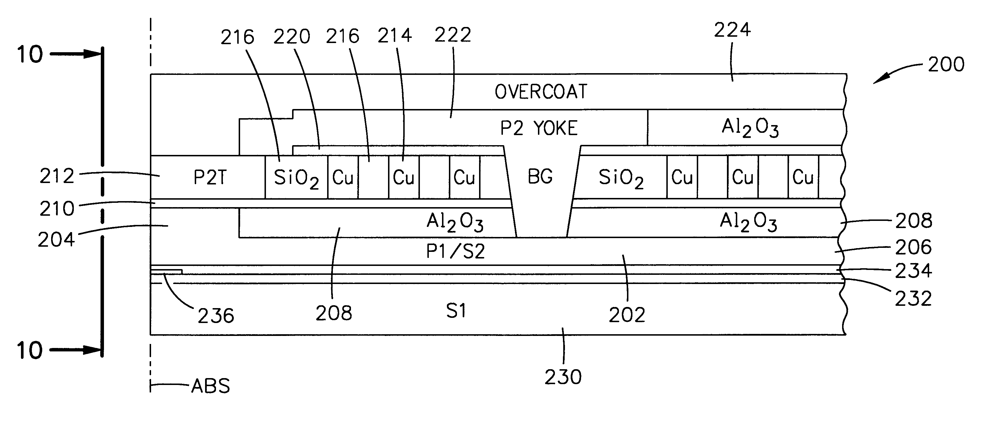
A method of making the first write head embodiment shown in FIGS. 9 and 10 is shown in FIGS. 13-28. In FIG. 13 a first pole piece material layer 300 is formed by any suitable means such as photopatterning with photoresist and plating. The first pole piece material layer 300 may be formed on the second read gap layer 234 shown in FIG. 9. The left side of the first pole piece material layer 300 is an air bearing surface (ABS) site which is formed after all of the heads are completed on a wafer and diced into rows of heads. Accordingly, the first pole piece material layer 300 actually covers an entire wafer and then is subsequently processed, which will be described next.
In FIG. 14 the first pole piece layer 300 in FIG. 13 has been photopatterned and plated to provide a first pole piece 302 that has a pedestal portion 304 in a pole tip region and a recessed portion 306 which extends through the yoke region to at least the back gap (BG).
In FIG. 15 a rece...
PUM
| Property | Measurement | Unit |
|---|---|---|
| Thickness | aaaaa | aaaaa |
| Electrical conductivity | aaaaa | aaaaa |
| Ferromagnetism | aaaaa | aaaaa |
Abstract
Description
Claims
Application Information
 - R&D
- Intellectual Property
- Life Sciences
- Materials
- Tech Scout
- Unparalleled Data Quality
- Higher Quality Content
- 60% Fewer Hallucinations
Browse by: Latest US Patents, China's latest patents, Technical Efficacy Thesaurus, Application Domain, Technology Topic, Popular Technical Reports.
© 2025 PatSnap. All rights reserved.Legal|Privacy policy|Modern Slavery Act Transparency Statement|Sitemap|About US| Contact US: help@patsnap.com


