
Dual mode programmable delay element

a delay element and dual-mode technology, applied in the field of digital circuits, can solve the problems of increasing the complexity of digital processors, increasing the non-uniformity of signal propagation time, and finite signal propagation tim

Inactive Publication Date: 2001-04-24
IBM CORP
View PDF6 Cites 34 Cited by
  • Summary
  • Abstract
  • Description
  • Claims
  • Application Information

AI Technical Summary

Benefits of technology

It is another object of the invention to provide a programmable delay element capable of providing delays with a resolution of less than the propagation delay of a single, replicable, circuit.

Problems solved by technology

However, signal propagation time is necessarily finite and non-uniform due to capacitances and resistances of interconnections and other loads such as those presented by the gates of CMOS devices which are currently the logic circuit technology of choice for most digital circuits and the signal propagation time within the circuits, themselves.
The non-uniformity of signal propagation time has increased with digital processor complexity and burdensome design analyses are generally required to determine critical signal paths and maintain propagation time within tolerances in those critical paths.
Even non-critical paths may present problems and cause errors of logic function in relatively simple circuit configurations and which cannot be reliably predicted.
However, either such possibility would greatly reduce the operational speed of the overall logic circuit or processor.
Thorough design analysis and adjustment of propagation time of each node of each signal propagation path would be economically prohibitive and does not guarantee the performance of the circuit.
However, it should be appreciated that delay elements can consume significant amounts of chip space, depending on the maximum amount of delay to be accommodated.
Circuit designs capable of such a short set-up time are substantially more complex since they must internally measure signal propagation time through the delay element and immediately adjust the location at which the output is to be taken.
It is also necessary to provide equal delay from each tap of the delay line to the output of the multiplexer including the connections from the delay elements to the multiplexer inputs and accommodation of this requirement increases the complexity of the delay element design and requires unique layouts for delay elements of each different maximum delay to be produced.

Method used


Image

  • Dual mode programmable delay element
  • Dual mode programmable delay element
  • Dual mode programmable delay element

Examples


Embodiment Construction

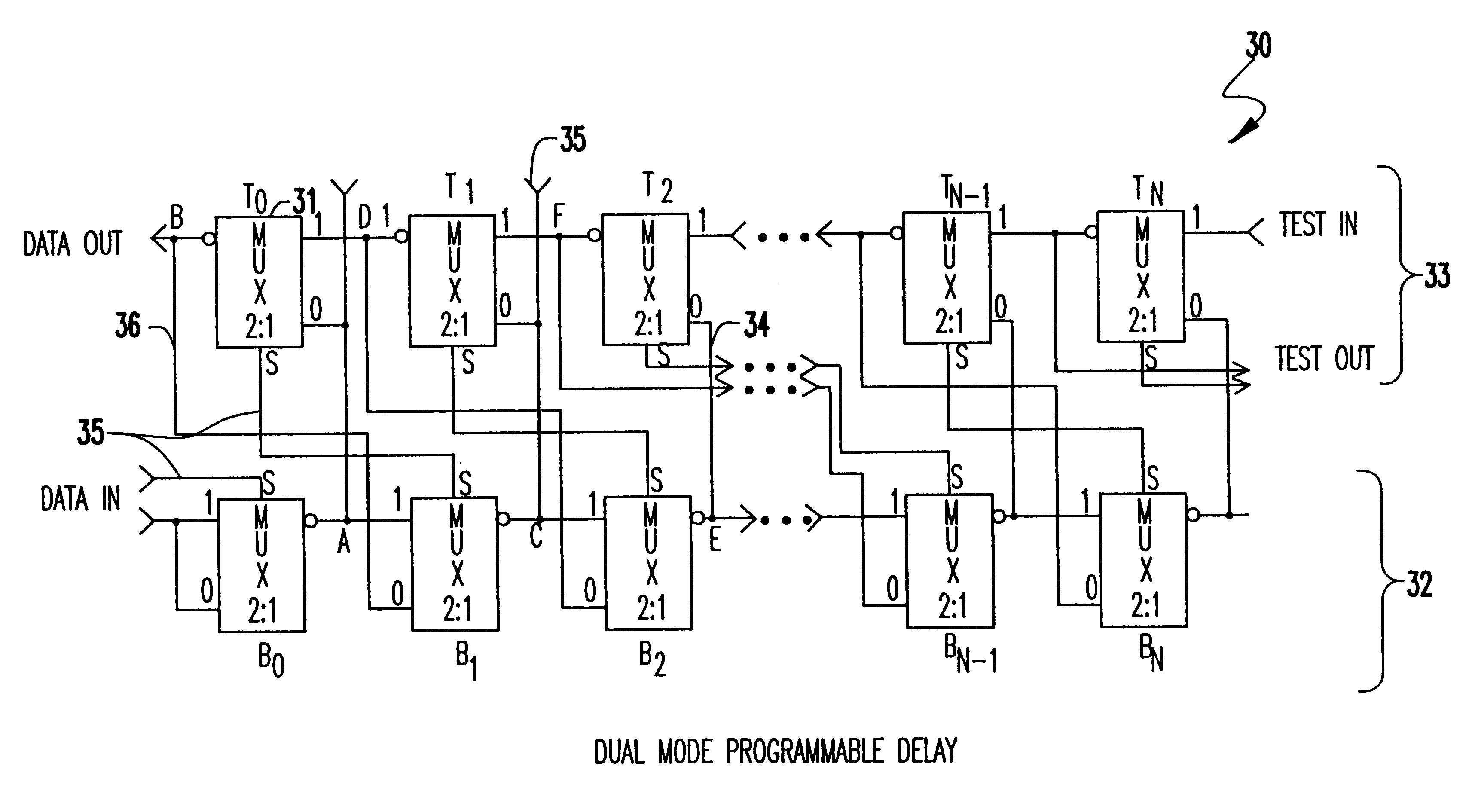
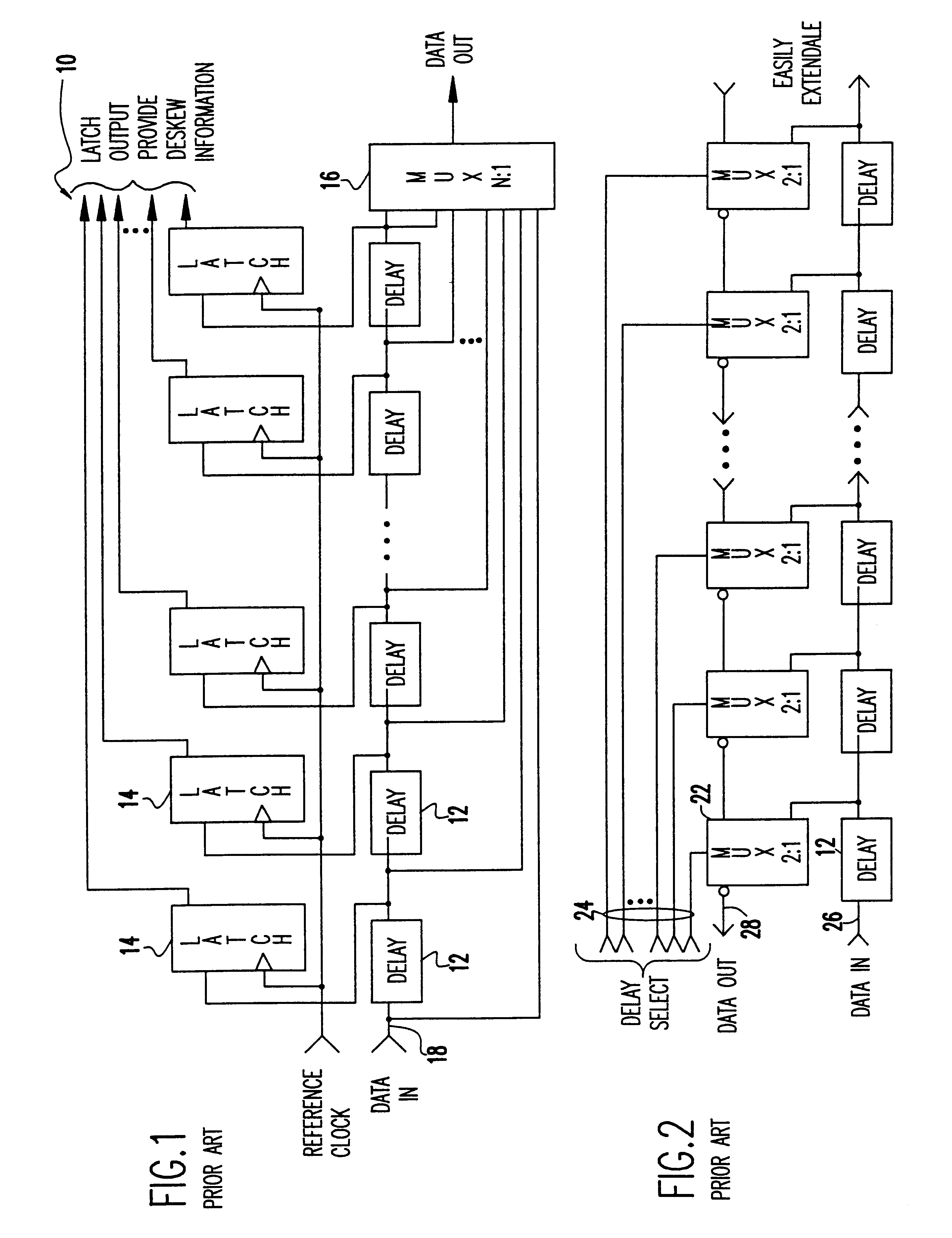
Referring now to the drawings, and more particularly to FIG. 1, there is schematically shown a representation of a conventional programmable delay element 10 exemplary of known delay elements supporting fast set-up time. In delay element designs of this type, a plurality of serially connected delay stages 12 with nodes connecting the delay stages (and, generally, the input and output) connected to respective inputs of multiplexer 16 which is controlled by outputs of latches 14.

In operation, a signal transition is launched into the serially connected delay stages 12 from input 18 with the inputs to latches 14 enabled. The inputs to the latches 14 are then disabled by a reference clock and the signal is stored in a latch (or plurality thereof) corresponding to the output of the delay stage 12 which the signal transition has reached. The output of the latch which indicates the signal transition thus controls the multiplexer 16 to select and connect the delay element output to the outpu...


PUM


Abstract

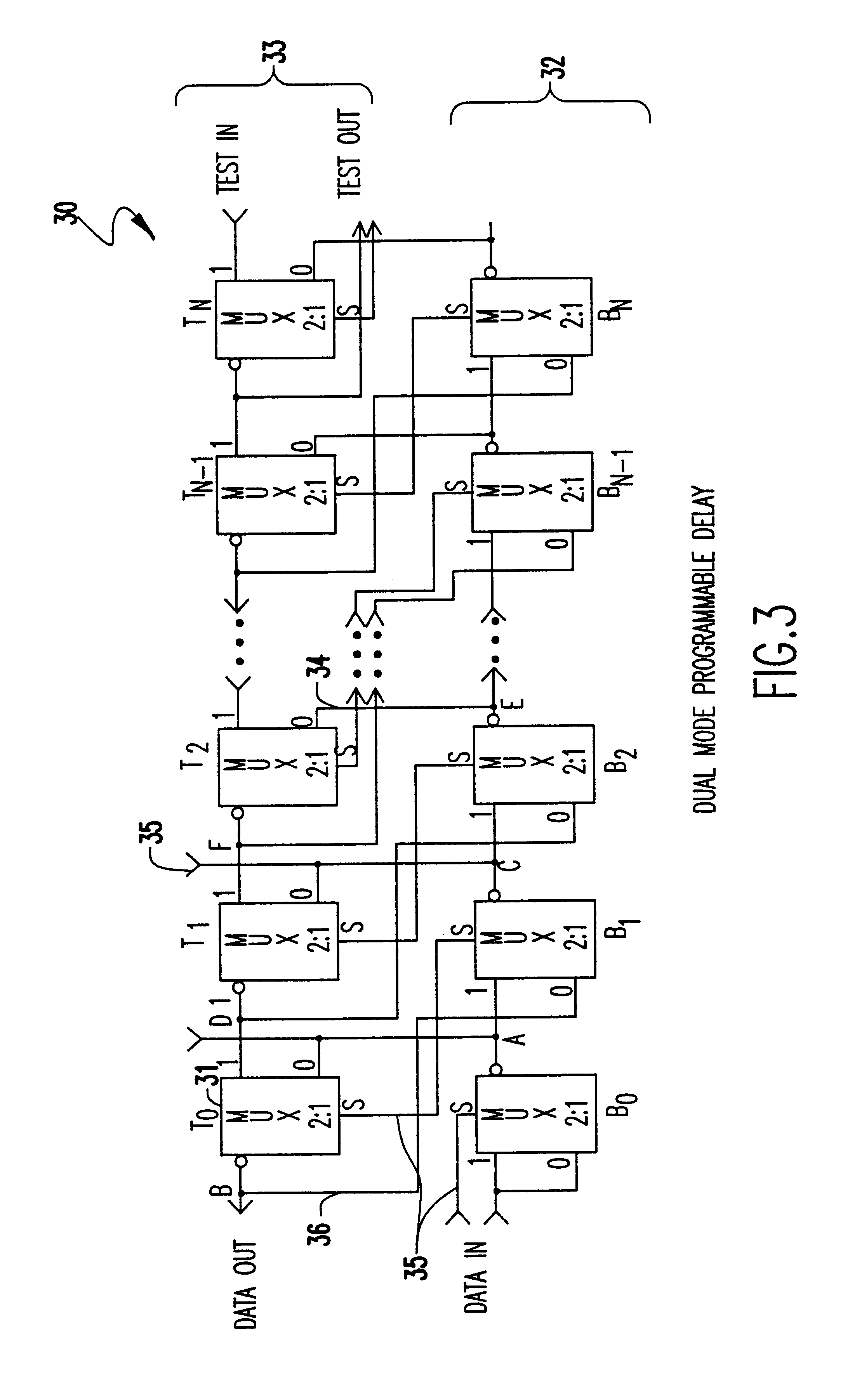
Rapid set-up is achieved in a programmable delay element having identical pairs of positionally corresponding delay stages in parallel arrays. The pairs of delay elements include identical arrangements of circuit elements and are replicable in a step-and-repeat fashion to simplify delay element manufacture for any arbitrary maximum delay time to be provided. Delay stages of the delay element are comprised of multiplexers. Outputs of respective delay stages are simultaneously stored as a signal transition is propagated through the delay stages in a first order to program the delay element. Thereafter, signals are propagated through selected delay stages in a second order controlled by the simultaneously stored outputs of respective delay stages during the propagation of the signal transition. The selected stages through which a signal is propagated in the second order are the same stages through which the signal transition had propagated in the first order at the time the delay stage outputs were simultaneously stored.

Description

1. Field of the InventionThe present invention generally relates to digital circuits for providing delay of digital signals and, more particularly, to programmable delay elements for correction and synchronization of propagation times of digital signals.2. Description of the Prior ArtModern digital logic circuits, such as those used in digital data processors, are characterized by short signal propagation times which are enhanced by decreased switching element (e.g. transistor) sizes and increased integration density. The short signal propagation times are exploited by reducing clock cycle times so that logic functions and data processing can be carried out more rapidly.However, signal propagation time is necessarily finite and non-uniform due to capacitances and resistances of interconnections and other loads such as those presented by the gates of CMOS devices which are currently the logic circuit technology of choice for most digital circuits and the signal propagation time withi...

Claims


Application Information

Patent Timeline
Patent Type & Authority Patents(United States)
IPC IPC(8): H03K5/13
CPCH03K5/131H03K5/133
Inventor GREGOR, ROGER PAUL
Owner IBM CORP
Learn More