
High bandwidth DRAM with low operating power modes

a high-bandwidth, dynamic random access memory technology, applied in the direction of memory adressing/allocation/relocation, instruments, sustainable buildings, etc., can solve the problems of memory being a system bottleneck, dram performance is a well-known limitation of computer system performance, and far short of processor performan

Inactive Publication Date: 2001-01-23
MARVELL ASIA PTE LTD
View PDF10 Cites 58 Cited by
  • Summary
  • Abstract
  • Description
  • Claims
  • Application Information

AI Technical Summary

Benefits of technology

It is therefore an object of the present invention to provide a high speed / narrow I / O dynamic random access memory (DRAM) which operates at a high bandwidth mode for accommodating, for example, graphic intensive applications, or in a low power mode for accommodating, for example, word processing or spreadsheet applications.
It is yet another object of the present invention to provide a high speed / narrow I / O DRAM where the speed / power mode can be adjusted to accommodate various applications.

Problems solved by technology

Dynamic random access memory (DRAM) performance is a well known limitation to computer system performance.
This is almost never the case and, so, the memory is a system bottleneck.
A high performance DRAM may have a 60 ns access time, which falls far short of processor performance.
This system bottleneck is exacerbated by the rise in popularity of multimedia applications.
However, SDRAMs and EDO RAMs still do not match processor performance and, therefore, still limit system performance.
The above high bandwidth approach achieves the high data rate by accessing a large number of bits in an array resulting in high power dissipation requirements.
For systems with a battery power option, this large power dissipation severely limits battery life.
This of course results in higher power requirements.

Method used


Image

  • High bandwidth DRAM with low operating power modes
  • High bandwidth DRAM with low operating power modes
  • High bandwidth DRAM with low operating power modes

Examples


Embodiment Construction

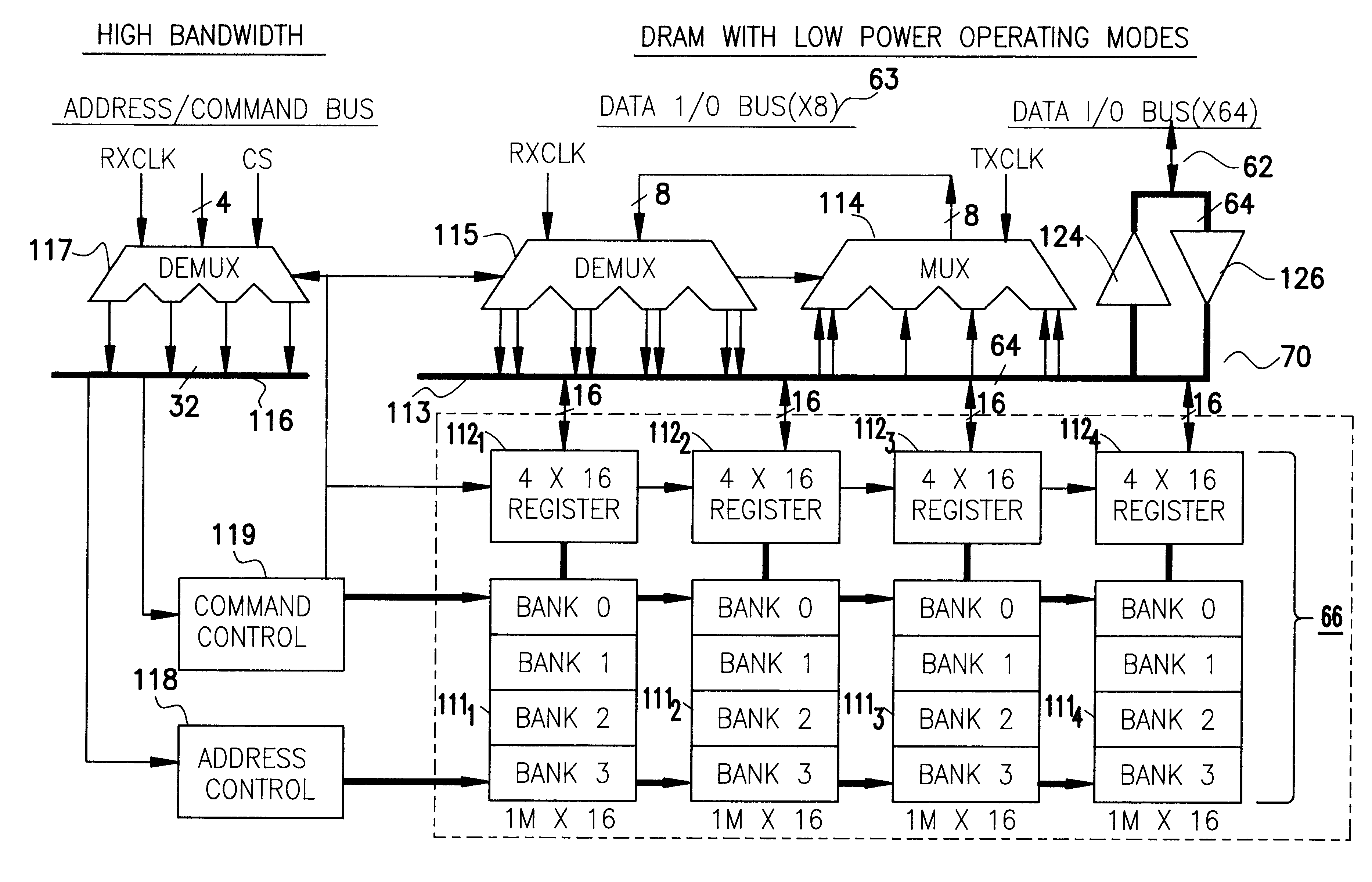
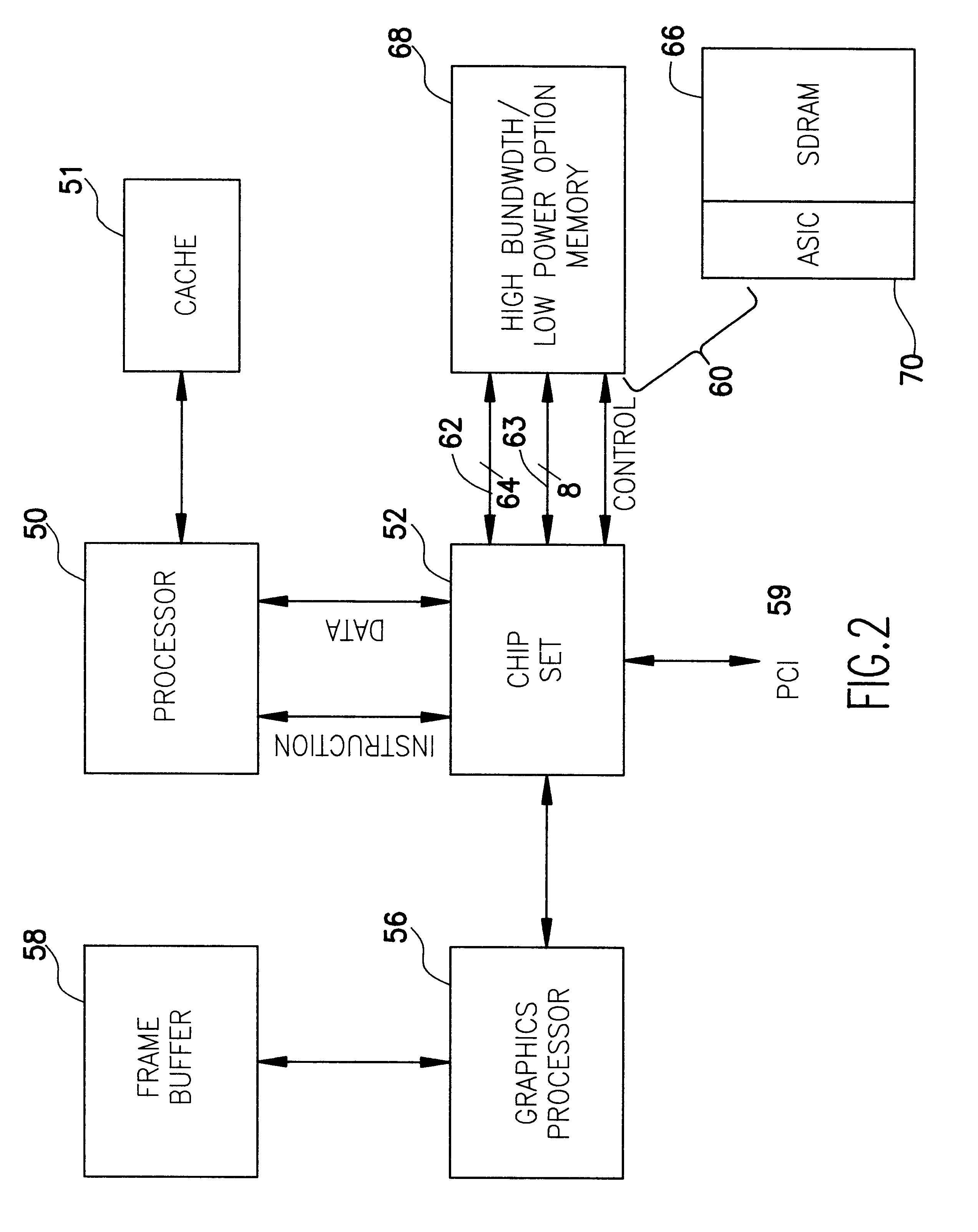
Referring now to the drawings, FIG. 2 shows a processor 50 and associated cache memory 51 connected to a chip set 52. The chip set is connected to a graphics processor 56 and a frame buffer 58 as well as a peripheral component interconnection bus (PCI) 59. The processor 50 is additionally connected to a dynamic random access memory (DRAM) 60. According to the invention, the DRAM 60 is selectively connected to the processor 50 via the chip set 52 by either a high-speed bus 63 or a slower, less power consuming bus 62. The chip set may be, for example, the INTEL PENTIUM 430, 440, or 450 series chipsets. The memory 60 may be, for example, a synchronous DRAM (SDRAM) 66 and application specific integrated circuit (ASIC) 70, as shown in FIG. 3 or a high-bandwidth DRAM 68 as shown in more detail in FIG. 4. In the case of an SDRAM 66 the application specific integrated circuit (ASIC) 70 is required to interface between the high speed bus 63 and the slower bus 62. In the case of a high-bandwi...


PUM


Abstract

A high bandwidth DRAM is provided with two separate bus networks connecting the DRAM to a processor. One bus network is a high speed (e.g., 500 MHZ) 8:1 or 16:1 multiplexed I / O bus and the second is a slower (e.g., 64-bit) bus. The high-speed bus is used for example for graphic intensive applications which require fast access to large numbers of bits in the DRAM memory array. This of course results in higher power requirements. Since, not all applications require such large amounts of data to be transferred between the DRAM and the processor, the slower bus is provided for these less demanding applications such as word processors, spreadsheets, and the like. The slower bus requires less power to operate and therefore results in a power saving mode which, among other things, facilitates longer battery life.

Description

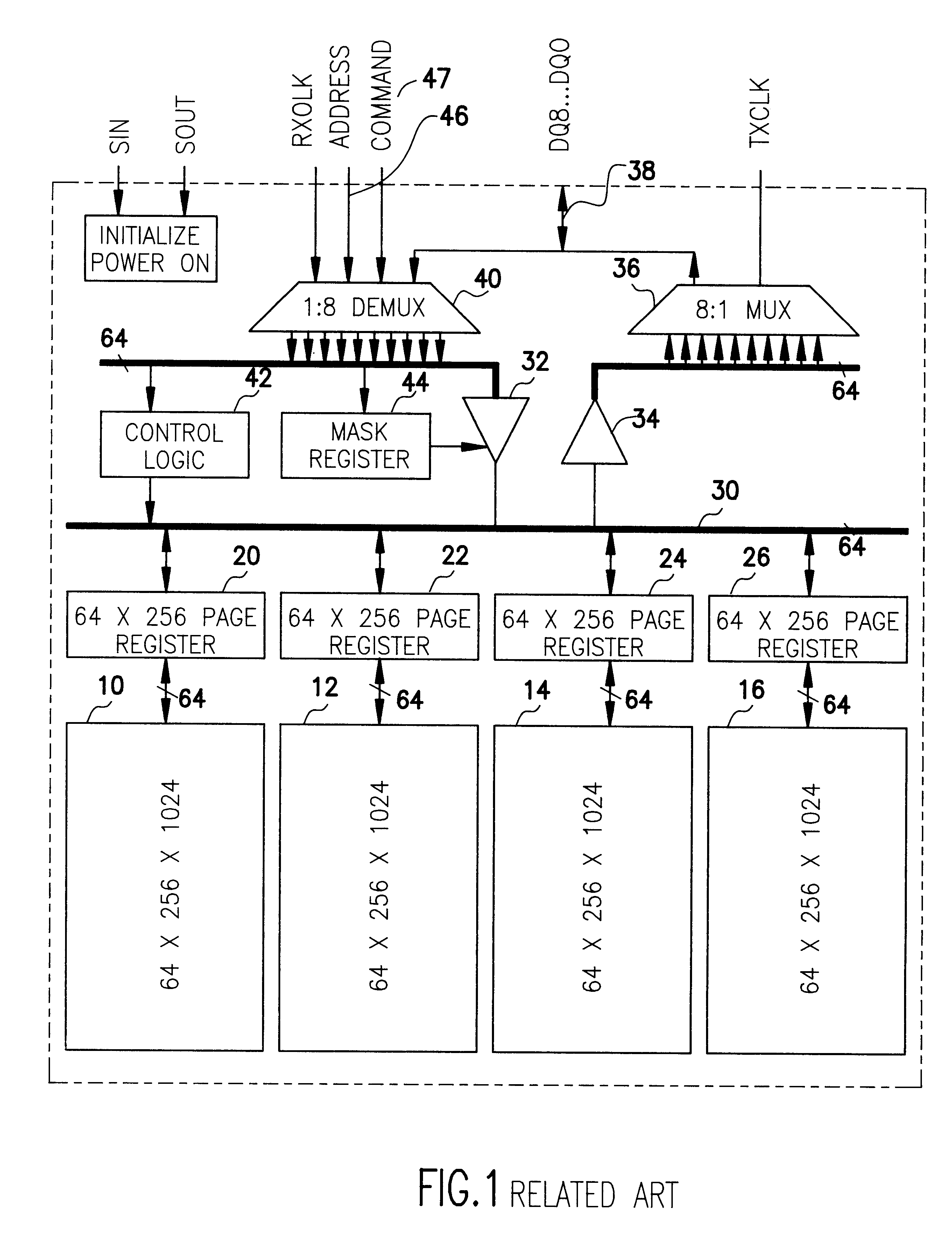
1. Field of the InventionThe present invention generally relates to high bandwidth / performance Dynamic Random Access Memories (DRAMs) and, more particularly, to high bandwidth / performance DRAMs with low power operating modes.2. Description of the Related ArtDynamic random access memory (DRAM) performance is a well known limitation to computer system performance. Processor speeds are rapidly outpacing main memory performance, with both processor designers and system manufacturers developing higher performance memory subsystems in an effort to minimize performance limitations due to the slower DRAM devices. Ideally, the memory performance would match or exceed processor performance, i.e., a memory cycle time would be less than one processor clock cycle. This is almost never the case and, so, the memory is a system bottleneck. For example, a state of the art high speed microprocessor may be based on a 200 MegaHertz (MHZ) clock with a 5 nanosecond (ns) clock period. A high performance D...

Claims


Application Information

Patent Timeline
Patent Type & Authority Patents(United States)
IPC IPC(8): G06F13/16G06F13/38
CPCG06F13/1684Y02B60/1228Y02D10/00G06F13/38
Inventor BERTIN, CLAUDE L.DELL, TIMOTHY J.HEDBERG, ERIK L.KELLOGG, MARK W.
Owner MARVELL ASIA PTE LTD
Learn More