Eureka AIR delivers breakthrough ideas for toughest innovation challenges, trusted by R&D personnel around the world.

Optical semiconductor light guide device having a low divergence emergent beam, application to fabry-perot and distributed feedback lasers

a technology of emergent beam and emergent beam, applied in the direction of semiconductor lasers, instruments, optical elements, etc., can solve the problems of reduced active device performance characteristics, less tolerance of geometrical variations, and devices suffering

Inactive Publication Date: 2000-10-31
FRANCE TELECOM SA
View PDF6 Cites 10 Cited by
  • Summary
  • Abstract
  • Description
  • Claims
  • Application Information

AI Technical Summary

Benefits of technology

The device according to the invention can be implemented in simple manner using conventional procedures.
The present invention makes it possible to obtain a semiconductor guide device able to supply a light beam with a small divergence, without suffering from the disadvantages of the aforementioned, known devices and making it possible to reduce said divergence.
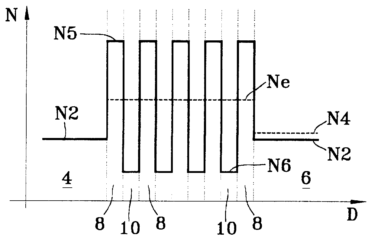
More particularly, for a core structure corresponding to a low mean refractive index, the effective index of the guide can be reduced, which gives rise to a limited confinement of the mode and to a reduction in the divergence of the beam emerging from the device.
A loss of a modal effect (e.g. absorption / gain / index) of an active device can be compensated, according to the invention, by increasing the overall volume of the core with high index layers and low index layers.
A device according to the invention makes it possible to obtain a beam divergence not exceeding approximately 10 to 15.degree., in both perpendicular directions, without using a mode adaption zone and using conventional double heterostructure amplifier or laser production procedures, such as BRS technology (two epitaxy stages, one standard photolithography stage and a chemical or dry etching for defining an active stripe having constant lateral and vertical dimensions).
Such a device has an a priori wide stripe making it possible to increase the geometrical tolerances. It is in particular well adapted to reduced divergence distributed feedback lasers as a result of the possibility of retaining a fixed width stripe throughout the device.

Problems solved by technology

However, the reduction of the stripe width (to values as small as 0.4 .mu.m) necessarily leads to a reduction in the performance characteristics of the active devices.
Moreover, not only are the submicron dimensions of the optimized stripe at the limit of the technological control possibilities, but also, for such a narrow guide, the characteristics of the component become less tolerant to geometrical variations.
The analysis of known semiconductor optical devices incorporating a light guide have a reduced divergence and use an integrated mode adaptor, revealing that such devices suffer from numerous disadvantages.
Compared with single function devices (laser, amplification, modulation), the addition of the mode adaptor requires the use of more complex manufacturing procedures with supplementary epitaxial growth stages (in all 4 to 5 stages) and also submicrometric stripe etching stages (often by expensive, direct writing with an electronic masker).
This has consequences on the manufacturing efficiency and therefore on the cost of the devices.
In particular, the geometrical tolerances of modal adaptors are often at the limit of technological possibilities, which reduces the control and reproducibility of the emission diagram.
The addition of a transition zone also generally produces a deterioration to the performance characteristics of the components, such as an increase in the operating currents, a power, amplification and absorption reduction, a disturbed emitted optical beam having minor lobes surrounding the major lobe, etc.
In order to ensure as gentle as possible an expansion of the guided mode (adiabatic transformation), the transition zone must have a length of approximately 200 to 400 .mu.m, which introduces supplementary propagation losses and increases the total length of the device to excessive values (approximately 600 to 800 .mu.m), thus reducing the manufacturing efficiency on a 2 inch semiconductor wafer (approximately 5 cm).
Moreover, in the particular case of DFB lasers, the transition zone induces significant disturbances in the longitudinal distribution of the injected charge carriers, known as hole burning, which gives rise to a deterioration of the spectral and dynamic behaviour of such lasers.

Method used


Image

  • Optical semiconductor light guide device having a low divergence emergent beam, application to fabry-perot and distributed feedback lasers
  • Optical semiconductor light guide device having a low divergence emergent beam, application to fabry-perot and distributed feedback lasers
  • Optical semiconductor light guide device having a low divergence emergent beam, application to fabry-perot and distributed feedback lasers

Examples


Embodiment Construction

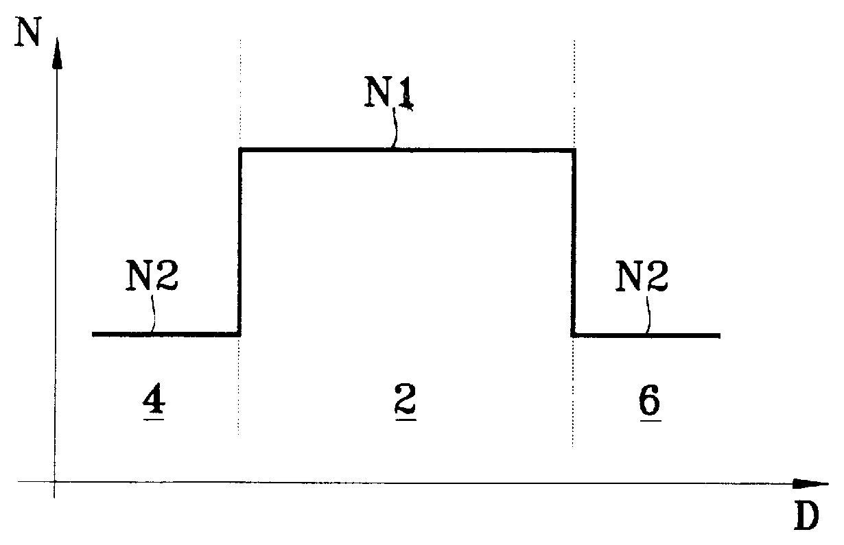
The present invention aims at obviating the aforementioned disadvantages by proposing an optical semiconductor light guide device in which the core of the guide comprises at least one layer, whose refractive index is high and fixed by the nature of the device (which can be a laser, a light amplifier, a light modulator or even a simple light guide) and at least one layer having a low refractive index, the latter being lower than the refractive index of each cladding layer of the guide or close thereto.

The guide core width is arbitrary in the present invention.

The device according to the invention can be implemented in simple manner using conventional procedures.

More specifically, the present invention relates to a semiconductor light guide device able to supply a small divergence light beam, the light guide having a core and cladding layers between which the core is positioned, said device being characterized in that the core of the guide comprises a group of semiconductor layers hav...


PUM


Abstract

Optical semiconductor light guide device having a low divergence emergent beam, application to Fabry-P+E,acu e+EE rot and distributed feedback lasers. According to the invention, the core of the guide of the device comprises at least one semiconductor layer (8), whose refractive index is higher than that of each of the confinement or cladding layers (4, 6) of the guide and at least one second semiconductor layer (10), whose refractive index is lower than that of each of the confinement or cladding layers or close thereto. Application to optical telecommunications.

Description

The present invention relates to an optical semiconductor light guide device with a low or small divergence emergent beam.It more particularly applies to the field of optical telecommunications and more especially transmissions by optical fibre at 1.3 and 1.5 .mu.m for subscriber service distribution applications.In order to generalize this type of optical link, it is vital to reduce the cost of the end optoelectronic components respecting the requirements of high performance, robustness and stability in the temperature range -40.degree. C. to +85.degree. C.An important part of the costs is due to assembly and fibre drawing operations, which at present are individual operations.An end component (optical head) essentially comprises a chip (e.g. having a laser amplifier, a modulator or a detector) and a fibre, which must be aligned and fixed in front of the active part of the chip.In the particular case of the laser, with a typical beam divergence of 30 to 40.degree., said operation r...

Claims


Application Information

Patent Timeline
IPC IPC(8): G02B6/122G02B6/30H01S5/20H01S5/00H01S5/34
CPCB82Y20/00G02B6/122G02B6/30H01S5/20H01S2301/18H01S5/2004H01S5/3421
Inventor OUGAZZADEN, ABDALLAHBOUADMA, NOUREDDINEKAZMIERSKI, CHRISTOPHE
Owner FRANCE TELECOM SA
Why Eureka
Eureka Blog
Learn More