Group III-nitride thin films grown using MBE and bismuth
a technology of nitride and bismuth, which is applied in the direction of single crystal growth, polycrystalline material growth, chemistry apparatus and processes, etc., can solve the problems of reduced carrier mobility of films made using conventional mbe technology, mbe films often exhibit a three-dimensional appearance, and limited crystal growth and grain sizes
- Summary
- Abstract
- Description
- Claims
- Application Information
AI Technical Summary
Benefits of technology
Problems solved by technology
Method used
Image
Examples
example 1
Undoped GaN films grown in the presence of Bi.
Substrates were prepared for deposition of the inventive optoelectronic GaN film by cleaning steps that followed a standard cleaning process. The substrates were degreased by boiling in acetone and ethyl alcohol for 5 minutes each and blown dry with nitrogen. After degassing in the load lock for 30 min at 500.degree. C., they were transferred into the growth chamber. The substrates were then heated up to 700.degree. C. for thermal desorption of surface contaminants. At this temperature, they were exposed to activated nitrogen for 10 minutes. Subsequently, a thin, low-temperature GaN buffer layer (.about.250 .ANG.) was deposited on the substrate. Its particular thickness was determined and optimized to minimize the strain (Kisielowski, C. et al., Phys. Rev BII 54, 17745, 1996); M. S. H. Leung et al. Mat. Res. Symp. Proc. 449, 1997, p 221 and H. Fujii et al. Mat. Res. Symp. Proc. 449, 1997, p.227); these three references incorporated herei...
example 2
Mg-doped GaN films grown in the presence of Bi.
Films were prepared as described above, using, in addition, Knudsen cells to evaporate Mg (99.99% pure).
Magnesium (Mg) doped GaN thin films grown in the presence of Bi (T.sub.Bi =350.degree. C. and T.sub.Mg =280.degree. C.) exhibited crystal sizes that compared well with those of the unintentionally doped n-type films described above. Unexpectedly, the size of the surface features, which corresponded to two-dimensional crystal size, increased significantly to about 10 .mu.m in diameter when Bi surfactant was used from a 623 K source. When the temperature was increased, The background impurity concentration was kept low and the intrinsic n-doping did not exceed 10.sup.17 cm.sup.3.
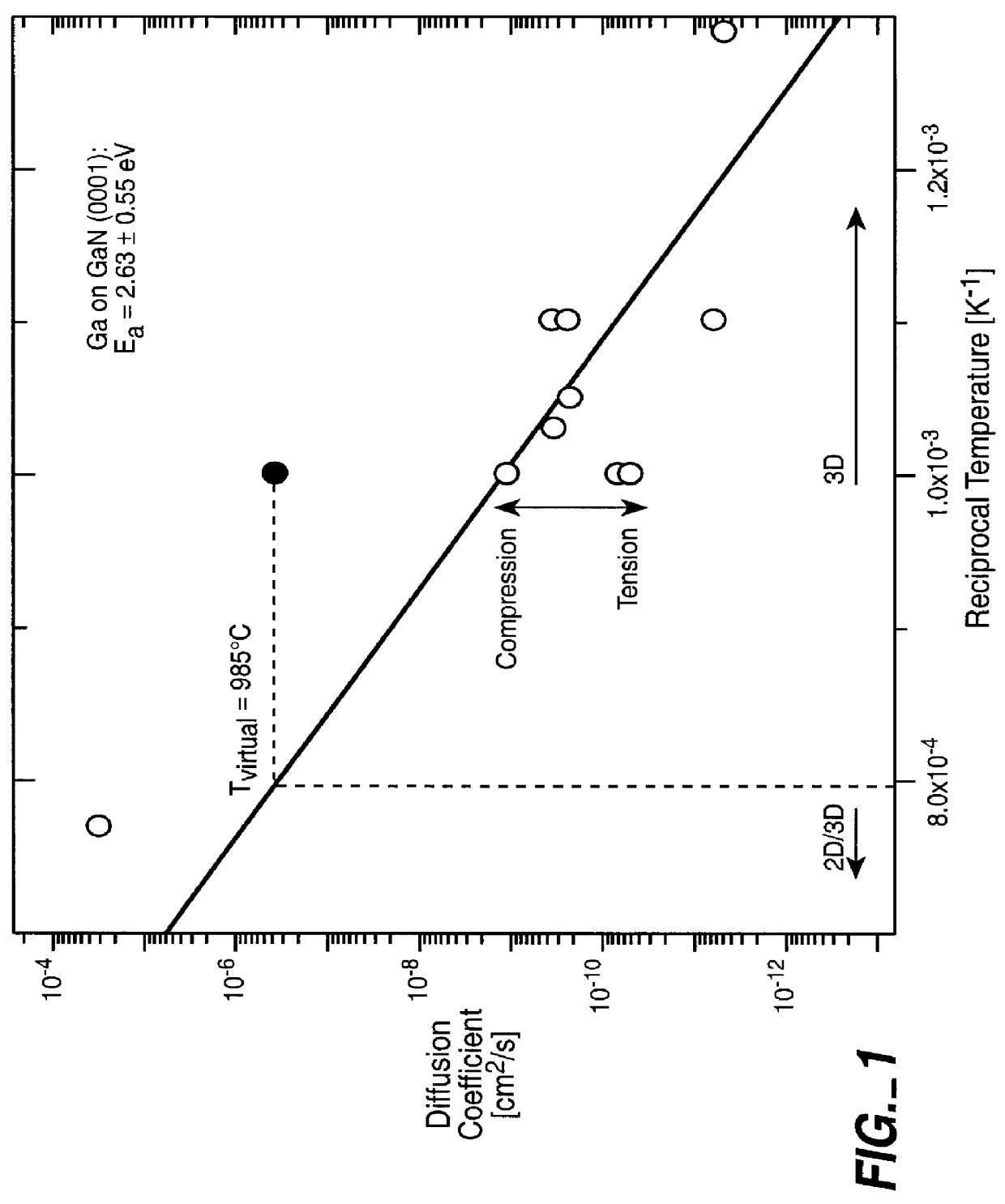
Previous experiments (Fujii et al., Ibid. 1997) suggested that the feature sizes that can be observed on the films relate to the size of oriented crystals which form the GaN thin films. This crystal size limitation was attributed to a temperature and strain depe...
example 3
Lateral Overgrowth of III-N films
Lateral overgrowth is a technique currently used in MOCVD-grown films to obtain regular grain sizes and shapes having low defect densities like dislocations or grain boundaries. For lateral overgrowth to work, the lateral growth rate of the film must exceed the vertical growth rate.
A substrate such as a silicon, sapphire, silicon carbide, germanium, gallium nitride, gallium arsenide, or other wafer is coated with, for example, an oxide layer, or a photoresist layer having about a thickness on the order of nanometers (nm). Grooves are etched in the layer. The groove dimensions are about 1 .mu.m wide and the spacing between the grooves is about twice the radius of the typical grain radius on an ungrooved surface.
The III-N film is first grown to fill the grooves, then continued growth takes place, overgrowing the grooves until the films growing out of each groove meet and coalesce in the middle of the space between the grooves and a continuous thin film...
PUM
 Abstract
Description
Claims
Application Information
 - R&D
- Intellectual Property
- Life Sciences
- Materials
- Tech Scout
- Unparalleled Data Quality
- Higher Quality Content
- 60% Fewer Hallucinations
Browse by: Latest US Patents, China's latest patents, Technical Efficacy Thesaurus, Application Domain, Technology Topic, Popular Technical Reports.
© 2025 PatSnap. All rights reserved.Legal|Privacy policy|Modern Slavery Act Transparency Statement|Sitemap|About US| Contact US: help@patsnap.com

