
Method for fabricating a self-aligned contact

Inactive Publication Date: 2000-10-24
TAIWAN SEMICON MFG CO LTD
View PDF9 Cites 19 Cited by
  • Summary
  • Abstract
  • Description
  • Claims
  • Application Information

AI Technical Summary

Benefits of technology

It is another object of the present invention to provide a method for forming a self-aligned contact with reduced susceptibility to the keyhole problem.
It is another object of the present invention to provide a method for forming a self aligned contact with reduced susceptibility to contact a bit line shorting.
It is yet another object of the present invention to provide an economical and robust method for forming a self aligned contact.
To accomplish the above objectives, the present invention provides a method for forming a self-aligned contact wherein a dielectric layer is formed directly on a conductive structure according the present invention. The process begins by providing a semiconductor structure having a polysilicon conductive structure (such as a bit line) thereon. A conductive area is located on the semiconductor structure adjacent to the conductive structure and the semiconductor structure. A top hard mask layer is formed over the dielectric layer. A contact opening is formed in the top hard mask layer and the dielectric layer using an etch selective to oxide over polysilicon, thereby exposing the conductive area of the semiconductor structure adjacent to the conductive structure without etching through the conductive structure. A first lining dielectric layer is deposited on the sidewalls of the contact opening and on the contact area of the semiconductor structure. A second lining dielectric layer is formed over the first lining dielectric layer. A third lining dielectric layer is formed over the second lining layer. The first lining dielectric layer and the third lining dielectric layer are composed of a material having poor step coverage such as PECVD silicon oxide. The second lining dielectric layer is composed of a material having good etch selectively with respect to the first and third lining dielectric layers, such as silicon nitride. The third lining dielectric layer is anisotropically etched forming a second contact opening in the third lining dielectric layer over the contact area while leaving a spacer on the sidewall of the contact opening. The second lining dielectric layer and the first lining dielectric layer are anisotropically etched to expose the conductive area of the semiconductor structure, while the spacer prevents erosion of the second lining dielectric layer and the first lining dielectric layer on the sidewall of the contact opening. The remaining spacer is removed using a selective etch such as buffered HF dip for an oxide spacer. A polysilicon contact layer is formed on the second lining dielectric layer and on the contact area of the semiconductor structure.

Problems solved by technology

However, as device dimensions and die sizes continue to decrease for higher density, the gap between adjacent conductive structures becomes narrower.
Sidewall spacers make the gap even narrow, resulting in a high aspect ratio for photolithography which reduces accuracy.
Another problem is caused by an overhang of the dielectric layer.
As the gap width decreases the overhang of the dielectric layer can close the gap at the top before the gap is completely filled resulting in a void (or key hole) in the dielectric layer.
The short can result in cell failure.
Yet another problem which can occur in a self aligned contact process is silicon nitride etch through.
Over-etching can cause etch through of the hard mask and / or the sidewall spacer and an electrical short between the conductive structure and the adjacent self aligned contact.
(1) The conductive structure and hard mask with sidewall spacers cause a high aspect ratio making precise photolithography difficult.
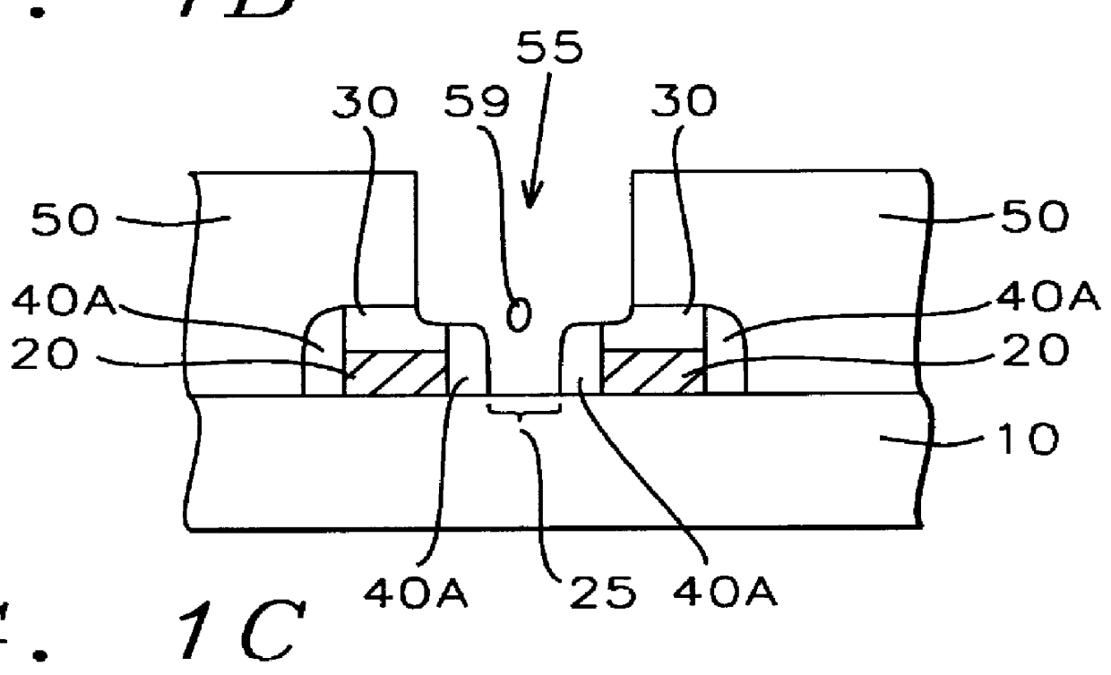
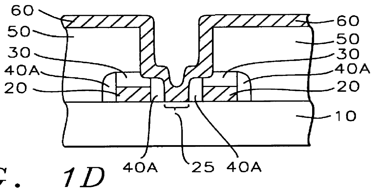
(2) poor gap filling in the narrow gap between adjacent conductive structures can cause a void (or key hole) in the inter poly oxide layer.
(3) Over etching during contact opening etch can cause etch through of the silicon nitride hard mask or silicon nitride sidewall spacers resulting in contact to conductive structure shorting.
When the gap width between adjacent conductive structures is small, further narrowing by the sidewall spacers and the combined height of the conductive structure and the hard mask can result in a high aspect ratio (height to width) causing reduced precision in the photolithography and etch processes.
PECVD oxide has poor gap filling properties causing it to overhang (become concave) on vertical surfaces.
Another key disadvantage of the problem process is that silicon nitride etch through can cause a conductive structure (20) to contact layer (60) short.
However, as discussed above, increasing the thickness of the hard mask (30) and the sidewall spacers (40A) can increase aspect ratio and key hole problems.

Method used


Image

  • Method for fabricating a self-aligned contact
  • Method for fabricating a self-aligned contact
  • Method for fabricating a self-aligned contact

Examples


Embodiment Construction

FIGS. 2A through 2F, show a process for forming a self-aligned contact wherein the IPO layer is formed directly on a conductive structure according the present invention. The process of the present invention provides a reduced aspect ratio, a reduced key hole problem, and a reduced etch through problem.

In the preferred embodiment of the present invention, the process begins by providing a semiconductor structure (10), such as for a DRAM. As with the problem process, semiconductor structure is understood to include a substrate and possibly to include active and passive devices formed within the wafer and conductive and / or insulating layers formed over the substrate.

Referring to FIG. 2A, the semiconductor structure (10) has a conductive structure (20) thereon. A contact area (25) is located on the surface of the semiconductor structure (10) adjacent to the conductive structure (20). The conductive structure (20) is composed of polysilicon and has a thickness of between about 1000 Angs...


PUM


Abstract

A method for forming a self aligned contact wherein a dielectric layer is formed directly on a conductive structure according the present invention. A semiconductor structure having a polysilicon conductive structure (such as a bit line) thereon is provided. A contact area is located on the semiconductor structure adjacent to the conductive structure. A dielectric layer, preferably composed of silicon oxide is formed over the conductive structure and the semiconductor structure. A top hard mask layer is formed over the dielectric layer. A contact opening is formed in the top hard mask layer and the dielectric layer using an etch selective to oxide over polysilicon, thereby exposing the contact region of the semiconductor structure adjacent to the conductive structure without etching through the conductive structure. A first lining dielectric layer, a second lining dielectric layer, and a third lining dielectric layer are sequentially deposited on the sidewalls of the contact opening and on the contact area of the semiconductor structure. The first and third lining dielectric layers are preferably composed of silicon dioxide and the third lining dielectric layer is preferably composed of silicon nitride. The third lining dielectric layer is anisotropically etched forming a second contact opening in the second lining dielectric layer over the contact area while leaving a spacer on the sidewall of the contact opening. The second lining dielectric layer and the first lining dielectric layer are anisotropically etched to expose the contact area of the semiconductor structure, while the spacer prevents erosion of the second lining dielectric layer and the first lining dielectric layer on the sidewall of the contact opening. The remaining spacer is removed, preferably using a buffered HF dip. A polysilicon contact layer is formed on the second lining dielectric layer and on the contact area of the semiconductor structure.

Description

BACKGROUND OF INVENTION1) Field of the InventionThis invention relates generally to fabrication of semiconductor devices and more particularly to a process for forming a self-aligned polysilicon contact, with a reduced aspect ratio contact opening, reduced chance of keyhole problems, and reduced chance of contact to bit line shorting.2) Description of the Prior ArtThe use of self aligned contact (SAC) processes has resulted in higher performance, lower cost, and increased density in semiconductor devices. If a self-aligned contact process, spacers are formed on the sidewalls of conductive structures (such as gates or bit lines). A dielectric layer is formed over these conductive structures. A contact opening is etched through the dielectric layer. A conductive layer, such as for capacitor crowns, is formed over the conductive structures and in the contact opening. However, as device dimensions and die sizes continue to decrease for higher density, the gap between adjacent conductive...

Claims


Application Information

Patent Timeline
IPC IPC(8): H01L21/02H01L21/60H01L21/314
CPCH01L21/76897H01L21/76831H01L21/3144H01L21/022
Inventor LEE, YU-HUAWU, CHENG-MINGCHIANG, MING-HSIUNG
Owner TAIWAN SEMICON MFG CO LTD
Learn More