
Programmable application specific integrated circuit and logic cell

a logic cell and integrated circuit technology, applied in the field of application specific integrated circuits, can solve the problems of long development cycle, high non-recurring engineering cost, poor flexibility in implementing the required logic functions,

Inactive Publication Date: 2000-06-20
QUICKLOGIC
View PDF68 Cites 59 Cited by
  • Summary
  • Abstract
  • Description
  • Claims
  • Application Information

AI Technical Summary

Problems solved by technology

The gate array, standard cell, and full custom technologies offer high performance and flexibility, although at the expense of a long development cycle and a high non-recurring engineering cost.
Their utility has been limited in general due to a relatively low number of available usable gates, poor flexibility in implementing the required logic functions, low speed of operation, and high power consumption.
The reason for the limited utility of FPLA and PLD devices is generally due to the exponential increase in the size of the array as the number of logic elements increase.
Generally, such devices are resistive and high in parasitic capacitance, and consume a relatively large silicon area.
Since generally each product term consumes a certain amount of power, as the array size increases, the power dissipation increases.
Moreover, the speed decreases with increasing array size, due to the increasingly parasitic capacitance of the array.
Hence, for a given technology, the size of the array is restricted by practical considerations.
While some improvement in maximum practical size is realized, the degree of improvement is limited by the same problems afflicting PLDs and FPLAs; specifically, speed deterioration and power dissipation.
This device achieves a logic complexity of 300 2-input NAND gates.

Method used


Image

  • Programmable application specific integrated circuit and logic cell
  • Programmable application specific integrated circuit and logic cell
  • Programmable application specific integrated circuit and logic cell

Examples


Embodiment Construction

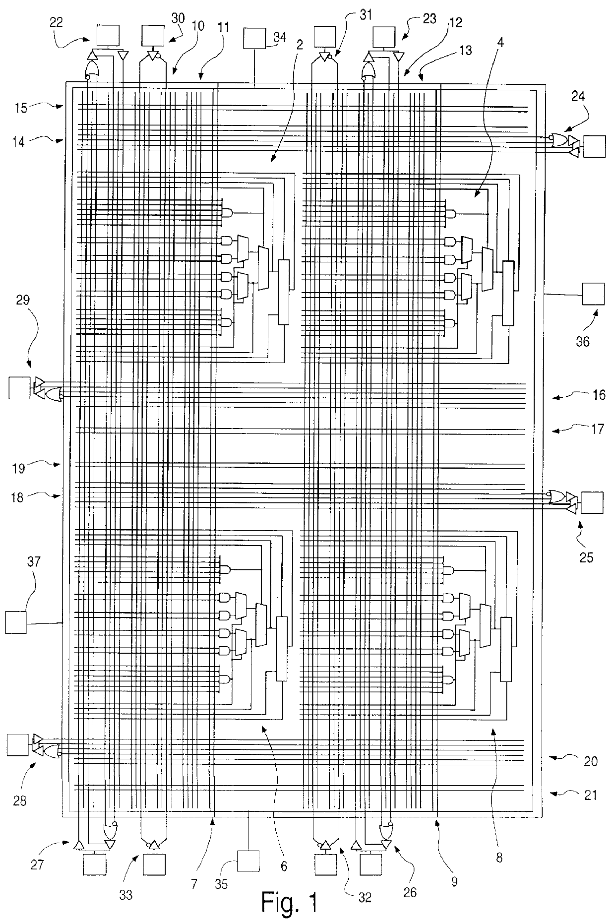
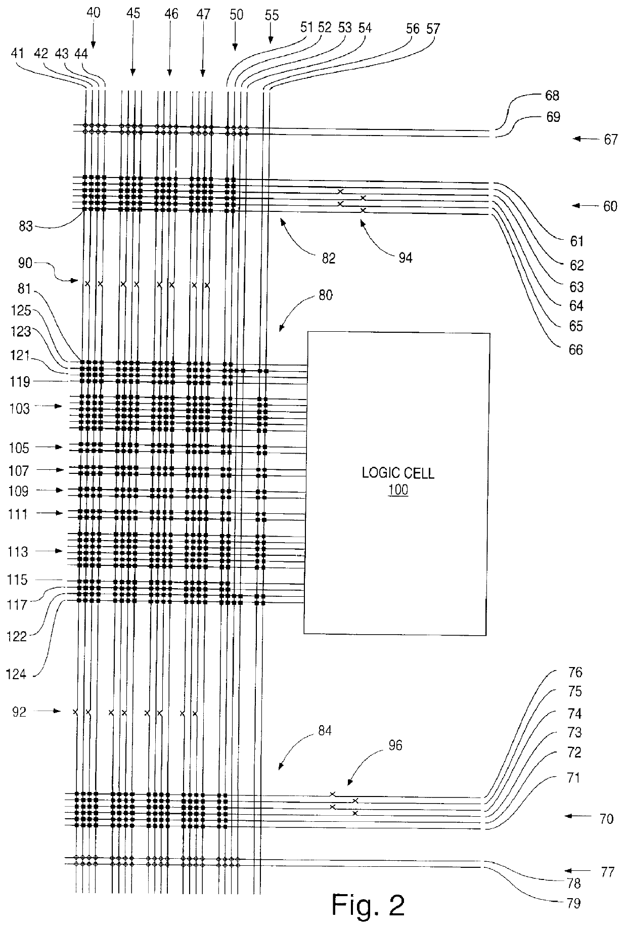
The routing and logic elements of an illustrative field programmable gate array having four logic cells is illustrated in FIG. 1. The field programmable gate array of FIG. 1 is configured as a 2.times.2 array of logic cells. A larger array may be achieved merely by extending the architectural features of the 2.times.2 array of FIG. 1 either horizontally or vertically, as desired. The array size of a practical field programmable gate array generally ranges from about 32 logic cells to about 1000 logic cells, depending on the application and the process technology used in fabrication.

A number of basic architectural features are illustrated, including logic cells 2, 4, 6, and 8; vertical wire segments 10, vertical express lines 11, and power lines 7 associated with a column of logic cells 2 and 6; vertical wire segments 12, vertical express lines 13, and power lines 9 associated with a column of logic cells 4 and 8; horizontal wire segments 14 and 16 and horizontal express lines 15 and...


PUM


Abstract

A field programmable gate array includes a programmable routing network, a programmable configuration network integrated with the programmable routing network; and a logic cell integrated with the programmable configuration network. The logic cell includes four two-input AND gates, two six-input AND gates, three multiplexers, and a delay flipflop. The logic cell is a powerful general purpose universal logic building block suitable for implementing most TTL and gate array macrolibrary functions. A considerable variety of functions are realizable with one cell delay, including combinational logic functions as wide as thirteen inputs, all boolean transfer functions for up to three inputs, and sequential flipflop functions such as T, JK and count with carry-in.

Description

1. Field of the InventionThe present invention relates to application specific integrated circuits, and more specifically to field programmable gate arrays and logic cells therefor.2. Description of Related ArtApplication specific integrated circuits ("ASIC") provide their users the ability to manufacture products having a proprietary design without having to begin the design at the device level. Many different ASIC technologies are available, including gate array, standard cell, full custom design, and programmable logic devices. The gate array, standard cell, and full custom technologies offer high performance and flexibility, although at the expense of a long development cycle and a high non-recurring engineering cost. Programmable logic devices, which include programmable logic array devices ("PLD") and field programmable logic array devices ("FPLA"), are useful in a variety of applications such as glue logic and simple integrated circuit designs. Their utility has been limited ...

Claims


Application Information

Patent Timeline
IPC IPC(8): H03K19/173H03K19/177H03K17/00H03K3/356
CPCH03K19/1737H03K19/17704H03K19/17728H03K19/17792H03K19/1774H03K19/1778H03K19/17736
Inventor CHAN, ANDREW K.BIRKNER, JOHN M.CHUA, HUA-THYE
Owner QUICKLOGIC
Learn More