
Millimeter wave module with an interconnect from an interior cavity

Inactive Publication Date: 2000-05-16
VEONEER US LLC
View PDF23 Cites 71 Cited by
  • Summary
  • Abstract
  • Description
  • Claims
  • Application Information

AI Technical Summary

Benefits of technology

Accordingly, it is a general object of the present invention to provide a packaged millimeter wave integrated circuit which is capable of efficient heat dissipation, capable of providing a complimenting CTE to the packaged millimeter wave circuit, and to provide at least one waveguide port for the efficient transfer of RF energy.

Problems solved by technology

The above-described ILCC package is not, however, appropriate for millimeter wave integrated circuits due to the frequency limitations of the use of molded packaging and surface mount attachment in a printed wiring board assembly.
Additionally, the ILCC exhibits inadequate heat removal capability and it does not provide a complimentary coefficient of temperature expansion (CTE) to the millimeter wave circuit packaged therein.

Method used


Image

  • Millimeter wave module with an interconnect from an interior cavity
  • Millimeter wave module with an interconnect from an interior cavity
  • Millimeter wave module with an interconnect from an interior cavity

Examples


Embodiment Construction

While the invention may be susceptible to embodiment in different forms, there is shown in the drawings, and herein will be described in detail, specific embodiments with the understanding that the present disclosure is to be considered an exemplification of the principles of the invention, and is not intended to limit the invention to that as illustrated and described herein.

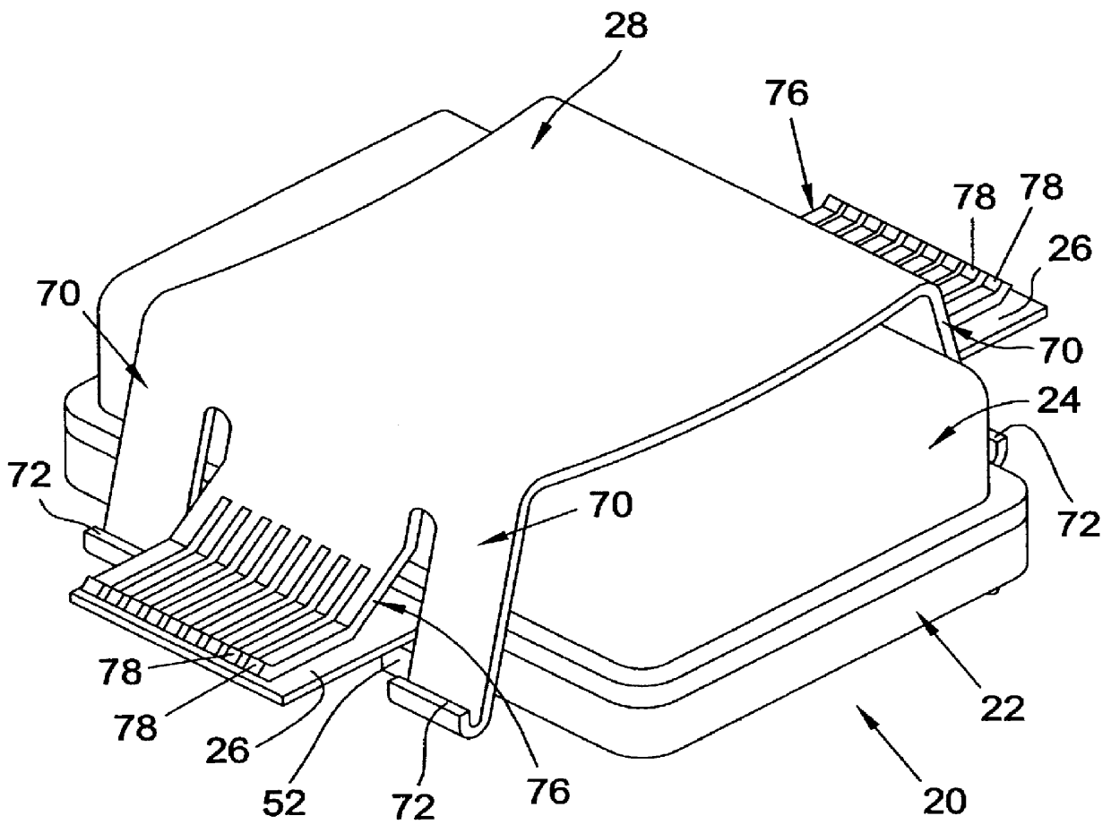
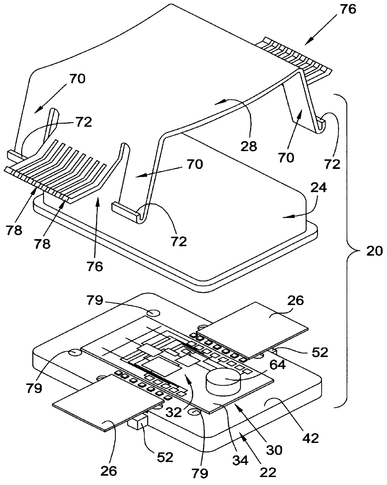
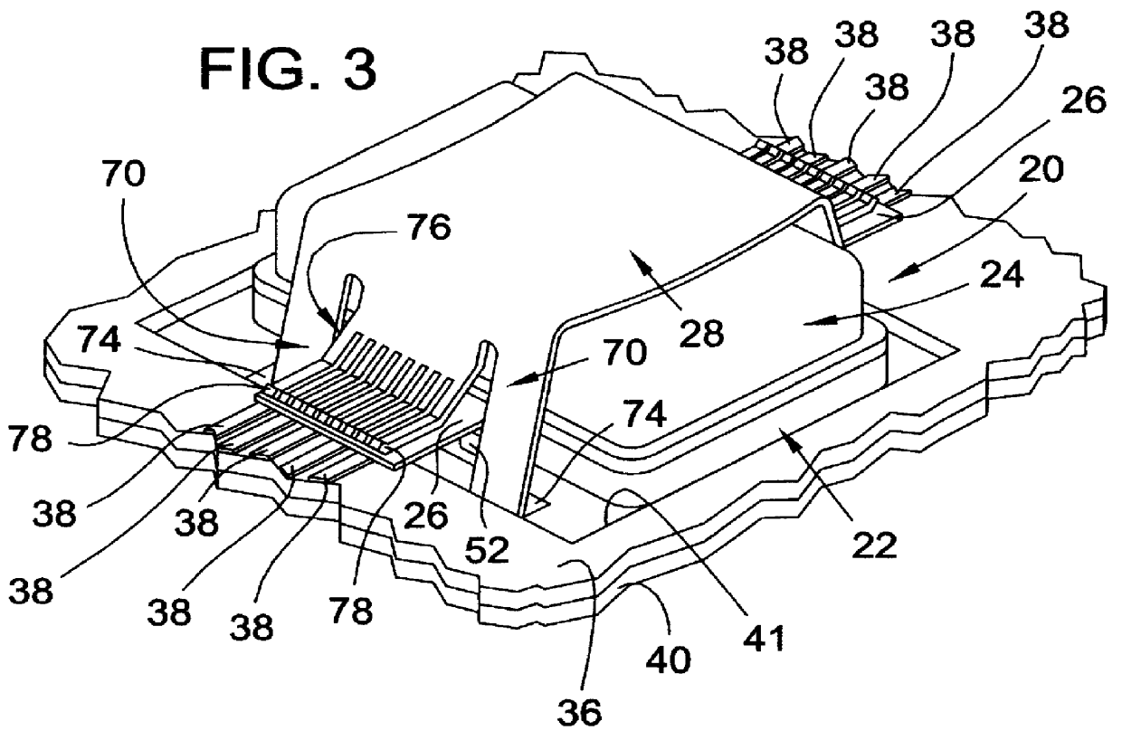
FIG. 1 illustrates a packaged integrated circuit 20 which is in accordance with a preferred embodiment of the present invention, and FIGS. 9 and 13 illustrate packaged integrated circuits 20a, 20b which are in accordance with alternative embodiments of the present invention. Each of the packaged integrated circuits 20, 20a, 20b will be hereinafter sometimes referred to as a "package". The package 20 which is illustrated in FIG. 1 and which is in accordance with a preferred embodiment of the present invention will now be described. FIGS. 1-9 relate to package 20.

As shown in FIGS. 1-3, the package 20 which is in ...


PUM


Abstract

A packaged integrated circuit (20, 20a, 20b) which includes at least one waveguide port (44, 44a, 44b) and at least one interconnect (26, 26a, 26b) which is electrically connected to an integrated circuit (30, 30a, 30b).

Description

The present invention relates generally to packaged integrated circuits, and more specifically relates to a packaged integrated circuit which includes one or more waveguide ports.One known integrated circuit package has a layered lead structure comprising a transmission layer, an insulating layer, and a base layer. The base layer is a relatively thick layer of copper. The insulating layer is a polyimide dielectric layer laminated onto the base layer. The transmission layer consists of multiple copper foil conductive traces that have been patterned onto the insulating layer. Such a laminated structure is commercially available from Mitsui Toatsu Chemicals Inc. under the trademark KOOL-BASE.RTM..The layered lead structure is press formed to have radiused ends on a perimeter thereof. The lead structure retains its shape due to the strength and memory of the copper base layer. The press form results in an indentation at a center of the lead structure. An IC is attached to the center and...

Claims


Application Information

Patent Timeline
IPC IPC(8): H01L23/66H01L23/58H01L23/40H01L23/02H01L25/04H01L25/18
CPCH01L23/66H01L2924/0002H01L2924/00
Inventor ZIEGNER, BERNHARD ALPHONSOSLETTEN, ROBERT JOHNJAIN, NITINBROWN, STEVE ROBERT
Owner VEONEER US LLC
Learn More