
Contact structure and electronic device having the same

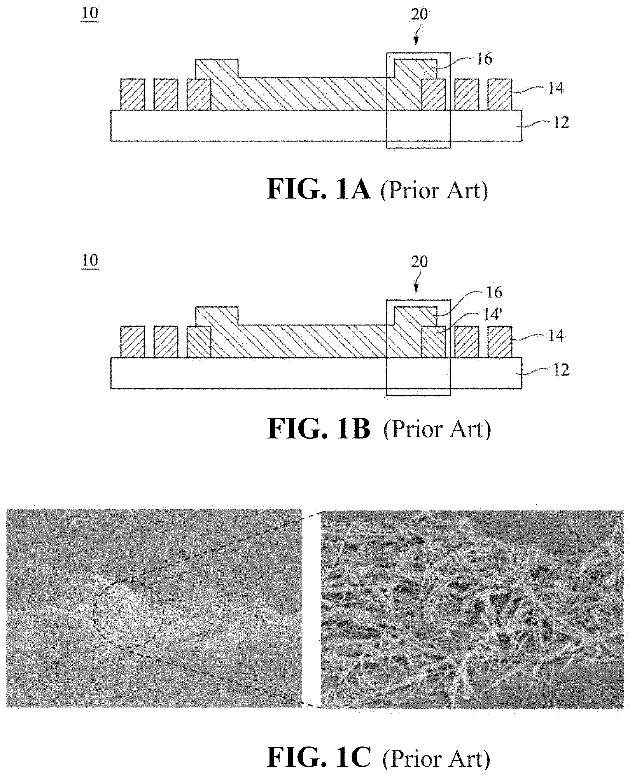
a technology of electronic devices and contact structures, applied in the direction of solid-state devices, semiconductor/solid-state device details, instruments, etc., can solve the problems of inability to meet the requirements for narrow bezel products, inability to complete etching in the etching process, and inability to reduce the interval between lines, etc., to achieve uniform distribution of silver nanowires

Active Publication Date: 2022-09-29
TPK ADVANCED SOLUTIONS
View PDF3 Cites 0 Cited by
  • Summary
  • Abstract
  • Description
  • Claims
  • Application Information

AI Technical Summary

Benefits of technology

The present disclosure provides a way to improve the distribution of nanowires on a copper layer in a stacked structure. By adding a layer that promotes the distribution of nanowires, incomplete etching and aggregation of nanowires are prevented. This results in more uniform etching and the ability to create finer line widths and intervals.

Problems solved by technology

However, there are problems of aggregation and poor distribution for silver nanowire at the above-mentioned contact surface, thereby causing incomplete etching in the etching process for this contact area.
Due to the incomplete etching of lines, the intervals between the lines cannot be reduced, and the requirement for narrow bezel products cannot be met.
For example, products with a line width<50 nm are prone to etching residues, which cause the condition of electrical abnormalities (such as short circuits).

Method used


Image

  • Contact structure and electronic device having the same
  • Contact structure and electronic device having the same
  • Contact structure and electronic device having the same

Examples


Embodiment Construction

[0028]The following disclosure provides different embodiments or examples to achieve different features of the above objectives. Specific examples of components and configurations are described below to simplify the present disclosure. These are, of course, examples only and are not intended to limit the present disclosure. For example, in the following description, the first feature is formed to be higher than the second feature, wherein an embodiment, in which the first and second features are formed to directly contact with each other, can be included; in addition, an embodiment, in which additional features are provided between the first and second features and thus the first and second features are not formed to directly contact with each other, can be included. In addition, in the present disclosure, numbers and / or letters may be repeatedly used as reference numeral in each example. Such repetition does not refer to the relationship between individual embodiments and / or config...


PUM

PropertyMeasurementUnit
diameteraaaaaaaaaa
thicknessaaaaaaaaaa
thicknessaaaaaaaaaa

Abstract

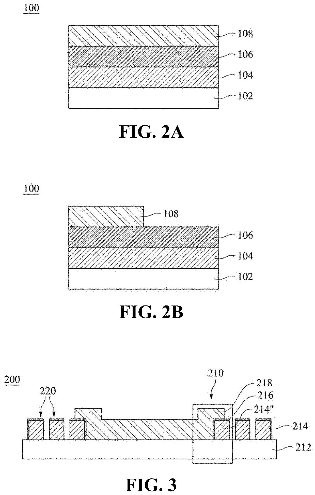
The present disclosure provides a contact structure and an electronic device having the same. The contact structure includes a substrate, a copper layer, an organic composite protective layer, and a silver nanowire layer. The copper layer is disposed on the substrate. The nanowire-distribution-promotion layer is disposed between the copper layer and the silver nanowire layer.

Description

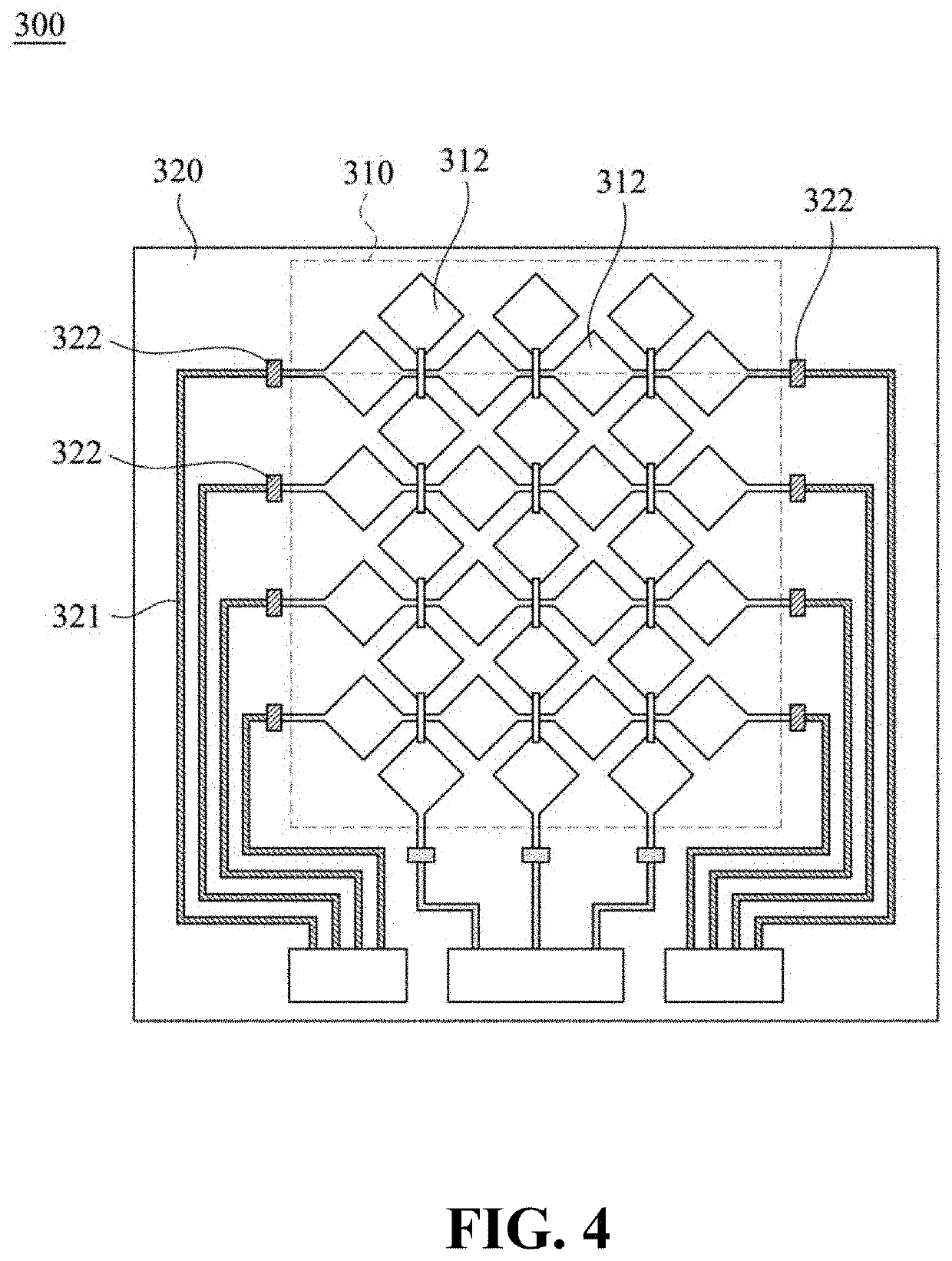
BACKGROUND1. Field of the Disclosure[0001]The present disclosure relates to a contact structure and an electronic device having the same, and more particularly, to a contact structure with stacked copper layer and silver nanowire layer, and an electronic device having the same.2. Related Art[0002]In the related art, in some electronic devices (such as touch panels), in the contact area where the touch electrode and the transmission line meet, a copper material layer is mostly used as the material of the transmission line, and a silver nanowire layer is used as the touch electrode. However, there are problems of aggregation and poor distribution for silver nanowire at the above-mentioned contact surface, thereby causing incomplete etching in the etching process for this contact area. Due to the incomplete etching of lines, the intervals between the lines cannot be reduced, and the requirement for narrow bezel products cannot be met.[0003]FIG. 1A shows a schematic diagram of a device ...

Claims


Application Information

Patent Timeline
Patent Type & Authority Applications(United States)
IPC IPC(8): G06F3/041H01L23/532
CPCG06F3/04164G06F3/0412H01L23/53238H01L23/53252H01L31/1888G06F3/0445G06F2203/04103G06F3/0443G06F3/0446
Inventor WANG, XI-ZHAOJIANG, YI-MINMU, LI-WEIWU, SHAN-YUKUO, CHAO-HUIZHAO, CAN-LIANGLIAN, HONG-YANLIU, CHUN-WEI
Owner TPK ADVANCED SOLUTIONS
Learn More