Production method of monocrystalline silicon

a monocrystalline silicon and production method technology, applied in the direction of crystal growth process, polycrystalline material growth, chemistry apparatus and processes, etc., can solve the problem of difficult cooling of monocrystalline silicon, deposits not completely removable by cleaning process, and literatures 1 and 2 cannot deal with a case where the emissivity declines beyond the set rang

Active Publication Date: 2022-05-26
SUMCO CORP
View PDF1 Cites 0 Cited by
  • Summary
  • Abstract
  • Description
  • Claims
  • Application Information

AI Technical Summary

Benefits of technology

[0032]According to the above aspects of the invention, the LPD failure on the silicon wafer due to the emissivity ε of the inner wall surface of the top chamber can be reduced.

Problems solved by technology

When the emissivity ε of the inner wall surface of the top chamber decreases, more heat is supplied from the inner wall surface of the top chamber to the monocrystalline silicon pulled up in the chamber, making it difficult to cool the monocrystalline silicon.
In addition, the deposits not completely removable by the cleaning process accumulate on the inner wall surface of the top chamber as the production batch is repeated.
However, the related arts disclosed in Patent Literatures 1 and 2 cannot deal with a case where the emissivity ε declines beyond the set range.

Method used


Image

  • Production method of monocrystalline silicon
  • Production method of monocrystalline silicon
  • Production method of monocrystalline silicon

Examples


first exemplary embodiment

[0070]A first exemplary embodiment of the invention will be described below with reference to the attached drawings.

Arrangement of Monocrystalline Silicon Production Machine 1

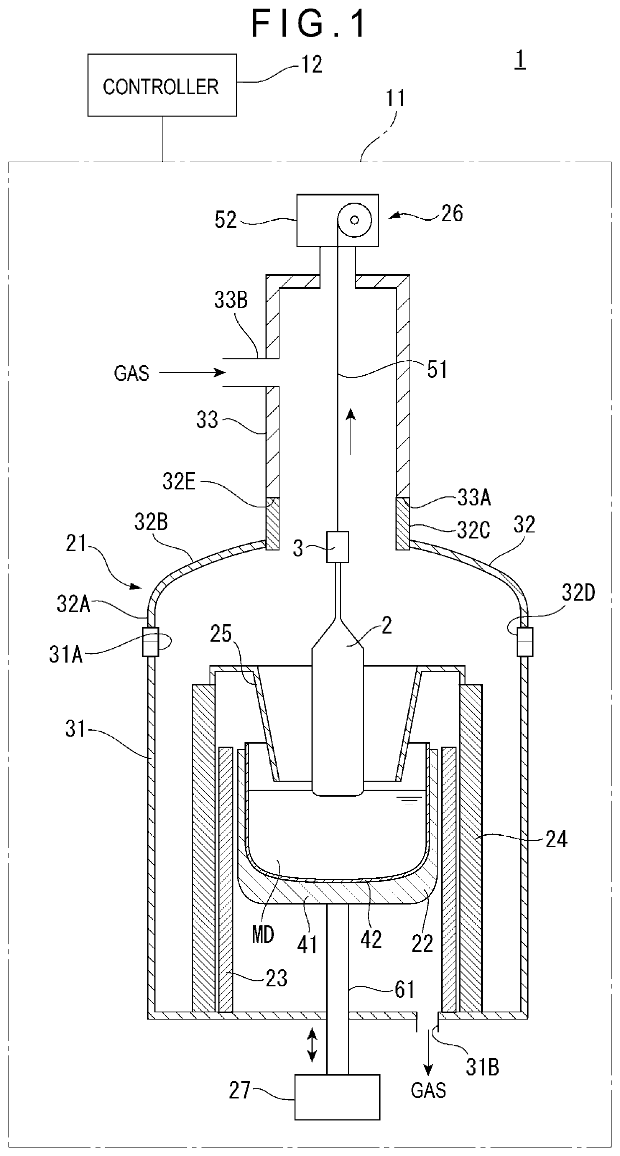
[0071]FIG. 1 is a schematic illustration of a monocrystalline silicon production machine 1 usable for a production method of monocrystalline silicon according to the first exemplary embodiment of the invention. The monocrystalline silicon production machine 1 is configured to produce the monocrystalline silicon 2 by the CZ method.

[0072]The monocrystalline silicon production machine 1 includes a machine body 11 and a controller 12. The machine body 11 includes a furnace body 21, a crucible 22, a heater 23, a heat insulation material 24, a heat shield 25, a pull-up unit 26, and a crucible driver 27.

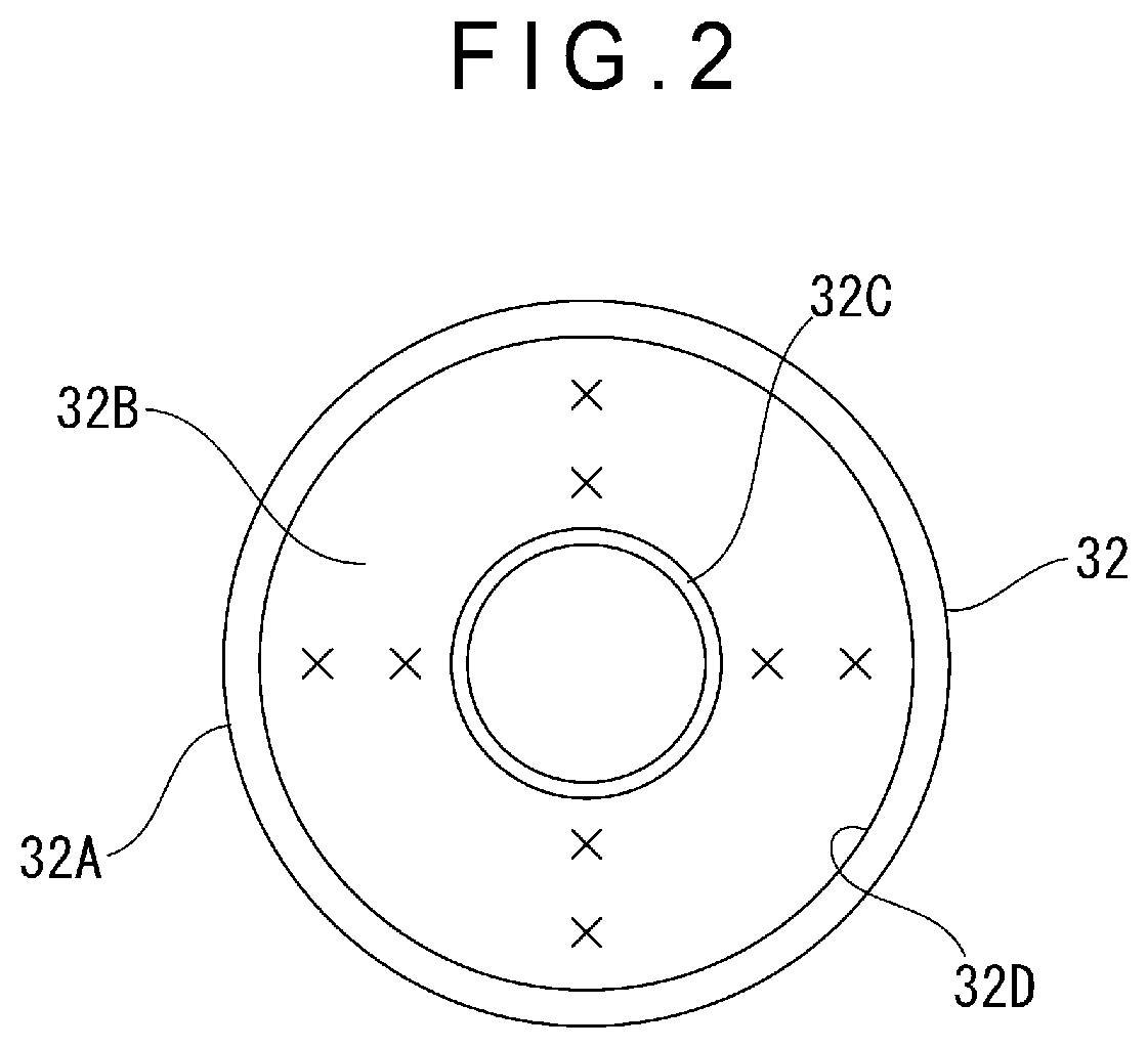
[0073]The furnace body 21 includes a main chamber 31, a top chamber 32, and a pull chamber 33. The main chamber 31 houses a crucible 22, a heater 23, a heat insulation material 24, and a heat shield 25. The crucible 22...

second exemplary embodiment

[0103]A second exemplary embodiment of the invention will be described below with reference to the attached drawings.

Arrangement of Monocrystalline Silicon Production Control System 100

[0104]FIG. 4 is a block diagram showing an exemplary arrangement of a monocrystalline silicon production control system 100 according to a second exemplary embodiment of the invention. The monocrystalline silicon production control system 100 includes a management machine 10 configured to control the production of monocrystalline silicon 2 in an entirety of a factory and respective controllers 12 of the monocrystalline silicon production machines 11 to 1n (n is a positive integer) connected to the management machine 10 via a network 9.

[0105]Each of the monocrystalline silicon production machines 11 to 1n used in the second exemplary embodiment, which are configured substantially in the same manner as the monocrystalline silicon production machine described in paragraphs 0057 to 0068 with reference to ...


PUM

PropertyMeasurementUnit
resistivityaaaaaaaaaa

Abstract

A production method of monocrystalline silicon includes: measuring an emissivity of an inner wall surface of a top chamber; and determining a target resistivity of monocrystalline silicon based on the emissivity measured in the measuring, thereby producing the monocrystalline silicon. In determining the target emissivity on a crystal center axis at a position for starting formation of a straight body of the monocrystalline silicon in the producing, when the emissivity is 0.4 or less, the target resistivity is determined to be less than a resistivity value of 3.0 mΩ·cm when the dopant is arsenic.

Description

[0001]The entire disclosure of Japanese Patent Application No. 2020-194828 filed Nov. 25, 2020 is expressly incorporated by reference herein.TECHNICAL FIELD[0002]The present invention relates to a production method of producing monocrystalline silicon by Czochralski method (abbreviated as “CZ method” hereinafter).BACKGROUND ART[0003]A low / mid voltage power MOSFET (Metal Oxide Semiconductor Field Effect Transistor), which is used as an electric-power device of a mobile device, has a predetermined intrinsic electric resistance (referred to as an “on-resistance” hereinafter) between a drain and a source when being powered on. Accordingly, the low / mid voltage power MOSFET by itself consumes power according to electric currents flowing therein while being powered on.[0004]Thus, the consumption power of the mobile device can be reduced if the on-resistance of the low / mid voltage power MOSFET can be reduced. Given such a background, there is a strong demand for monocrystalline silicon of l...

Claims


Application Information

Patent Timeline
Patent Type & Authority Applications(United States)
IPC IPC(8): C30B15/02C30B29/06C30B15/10C30B35/00
CPCC30B15/02C30B35/00C30B15/10C30B29/06C30B15/04C30B15/20C30B15/26
Inventor KAWAZOE, SHINICHIKOTOOKA, TOSHIROUTSUTSUMI, YUUJI
Owner SUMCO CORP
Why Eureka
Try Eureka