Printed Circuit Board Assembly Process Using Multiple Solders And Assembled Boards Made Using The Same

a printed circuit board and assembly process technology, applied in the field of electronic boards, can solve problems such as temperature-sensitive damage to components, achieve the effects of reducing the process step of solder reflow, reducing the cost of assembly, and ensuring the quality of assembly

Pending Publication Date: 2021-10-07
DELL PROD LP
View PDF13 Cites 6 Cited by
  • Summary
  • Abstract
  • Description
  • Claims
  • Application Information

AI Technical Summary

Benefits of technology

The patent describes a method for assembling electronic components on a printed circuit board using different solders and temperatures in separate steps. This allows for the attachment of components with different tolerances and compatibility characteristics to the same board without compromising the quality and reliability of other components. The method also reduces warping of the components during assembly and ensures proper and secure solder joints.

Problems solved by technology

For example, the most commonly used lead free solder paste alloy is SAC 305 which has a minimum reflow temperature (i.e., melting point temperature) of 220° C. and a peak process temperature of 260° C. This conventional board assembly process results in all of the components being attached to the PCB being subjected to process temperatures of 235° C. to 260° C. This reflow temperature range can cause damage to any component packages that are temperature-sensitive and cannot stand such temperatures, for example, due to excessive warpage and creation of open or low reliability solder joints at these temperatures.

Method used


Image

  • Printed Circuit Board Assembly Process Using Multiple Solders And Assembled Boards Made Using The Same
  • Printed Circuit Board Assembly Process Using Multiple Solders And Assembled Boards Made Using The Same
  • Printed Circuit Board Assembly Process Using Multiple Solders And Assembled Boards Made Using The Same

Examples


Embodiment Construction

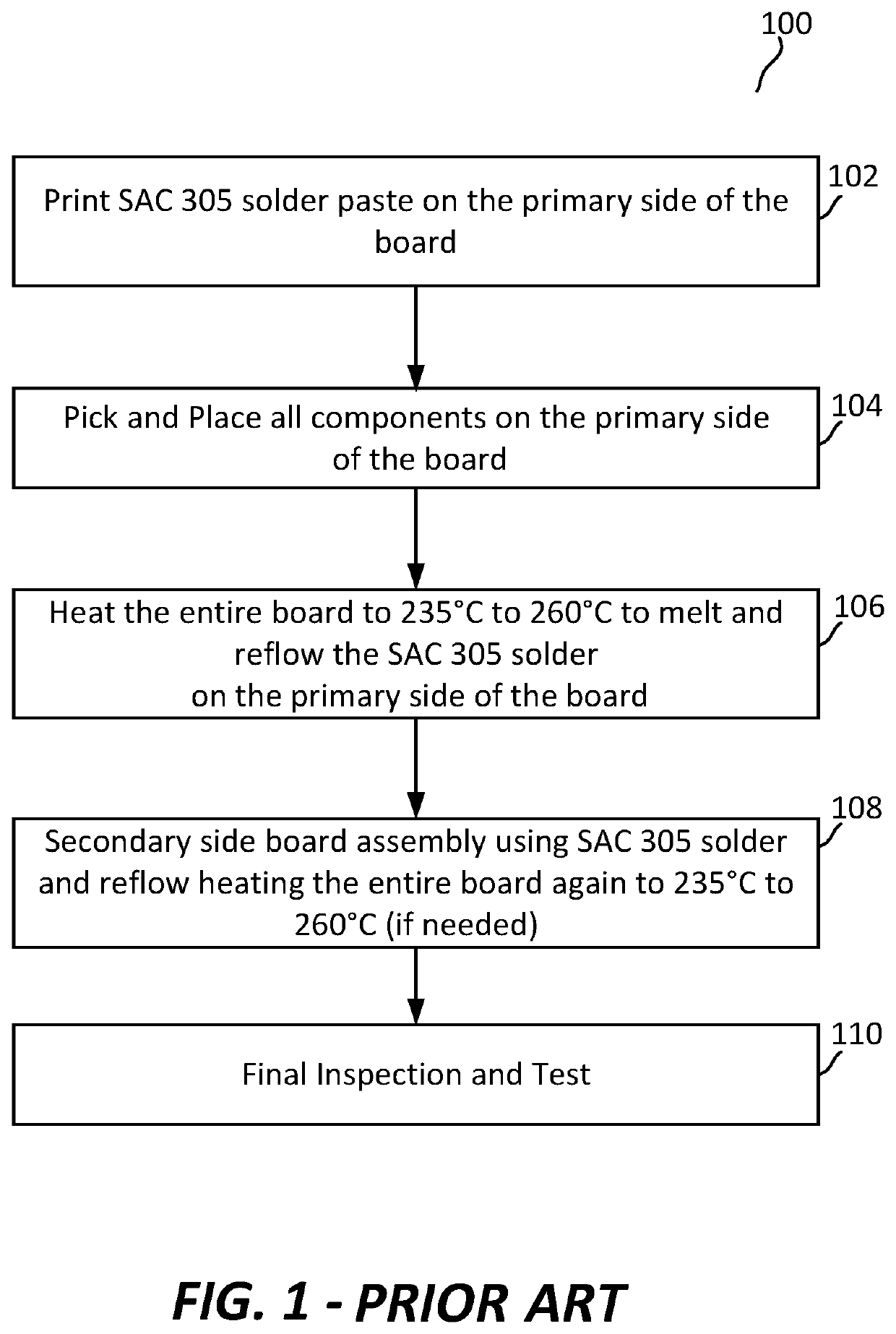
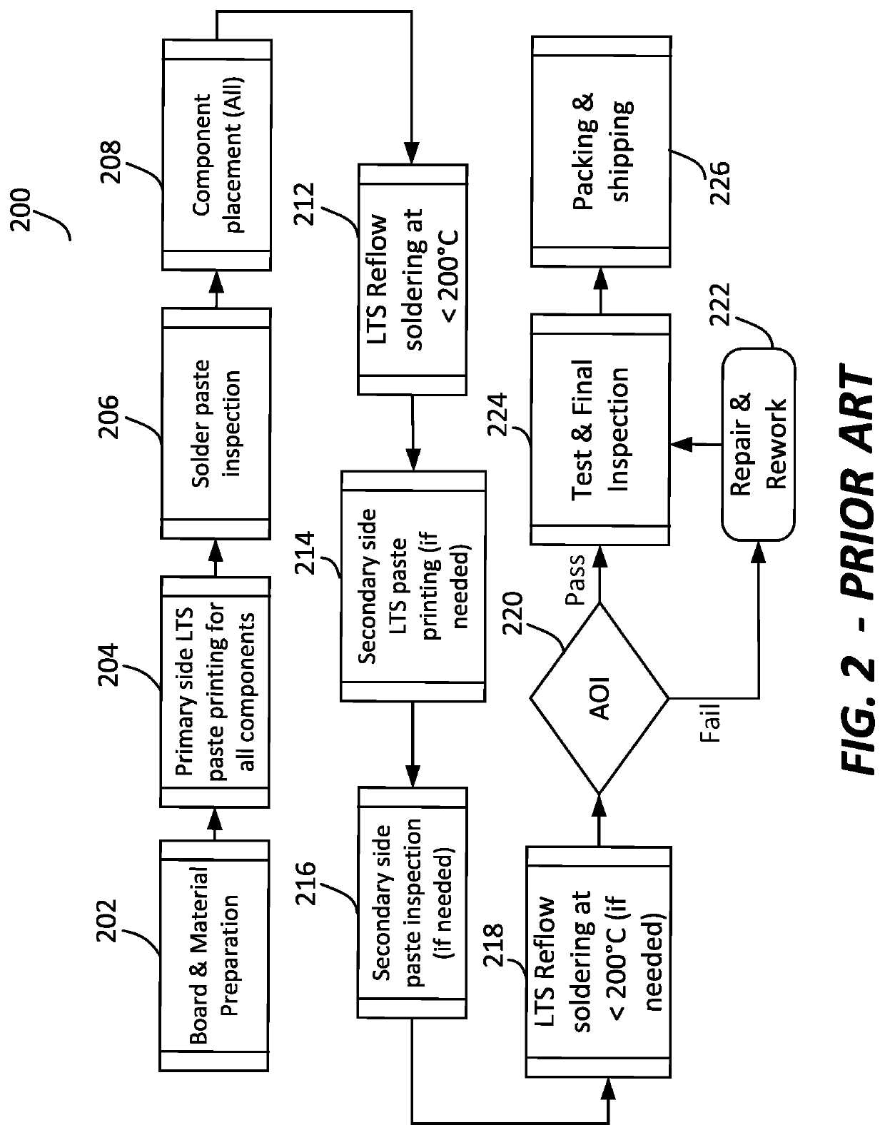
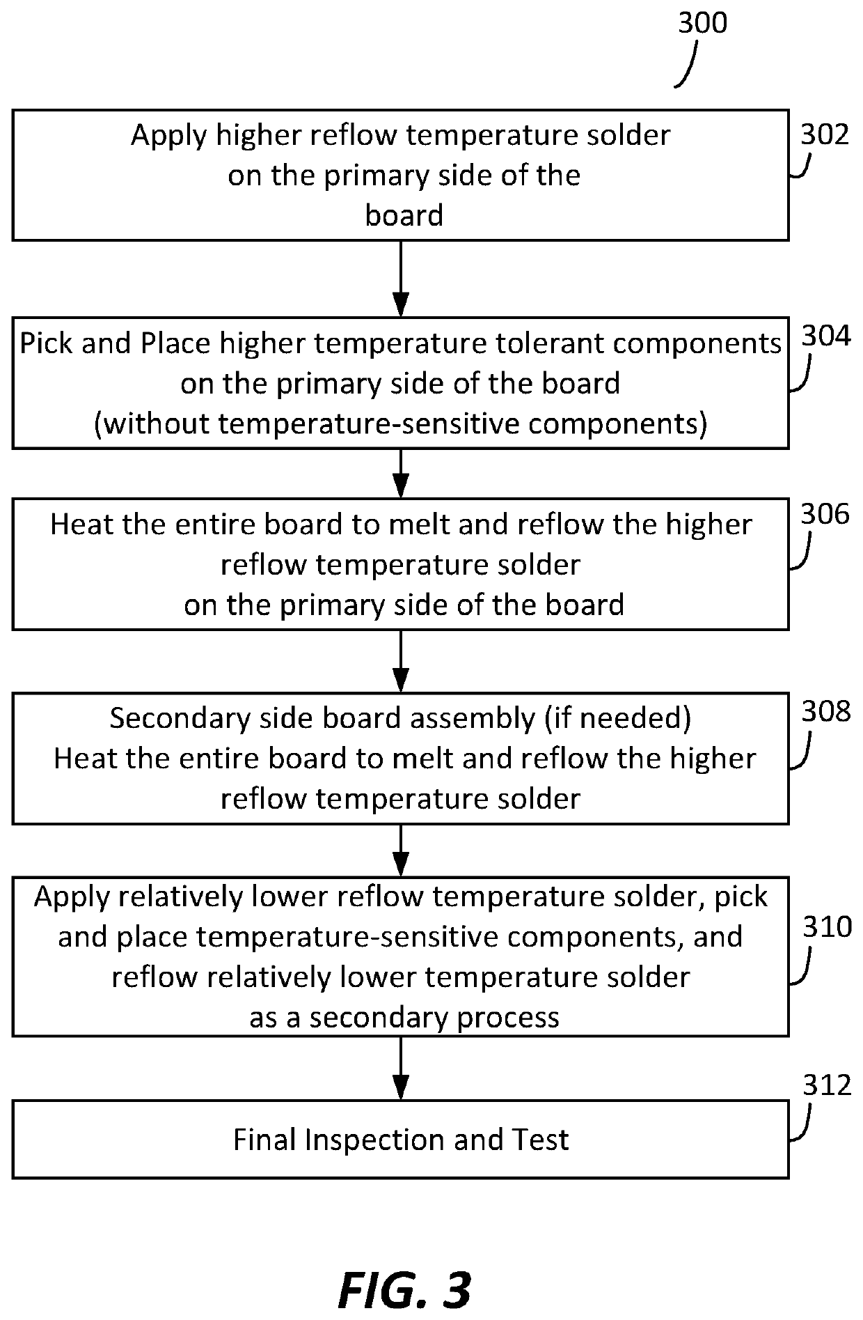
[0041]FIG. 3 illustrates one embodiment of a multiple step board assembly process flow 300 that may be implemented using a first relatively higher reflow temperature solder reflow process step to assemble higher temperature-tolerant electronic components to a PCB with relatively higher minimum reflow temperature (i.e., melting point temperature) solder (e.g., such as SAC 305), followed by a second relatively lower reflow temperature solder reflow process step to assemble one or more temperature-sensitive electronic components (e.g., such as a CPU BGA package or other type of electronic component package having temperature sensitivity) to the same PCB with a relatively lower minimum reflow temperature (i.e., melting point temperature) solder (e.g., LTS solder). Examples of CPU BGA packages include, but are not limited to, CPU BGA packages available from manufacturers such as Intel, Advanced Micro Devices (AMD), etc. Other types of electronic components may be BGA packages, packages h...


PUM

PropertyMeasurementUnit
Temperatureaaaaaaaaaa

Abstract

Board assembly processes are disclosed that may be implemented using multiple different electrically conductive solder types to assemble or attach different electronic components to a printed circuit board (PCB). For example, multiple different electronic components may be attached to a common PCB using a multiple-step assembly process that may be performed at different solder reflow temperatures and / or which may incorporate multiple different solder types having different respective minimum reflow temperatures (i.e., melting point temperatures). The disclosed processes may be implementing using a variety of different forms of solder, such as solder paste form, wire solder form, ingot solder form, etc.

Description

FIELD OF THE INVENTION[0001]This application relates to electronic boards and, more particularly, to board assembly processes.BACKGROUND[0002]As the value and use of information continues to increase, individuals and businesses seek additional ways to process and store information. One option available to human users is information handling systems. An information handling system generally processes, compiles, stores, and / or communicates information or data for business, personal, or other purposes thereby allowing human users to take advantage of the value of the information. Because technology and information handling needs and requirements vary between different human users or applications, information handling systems may also vary regarding what information is handled, how the information is handled, how much information is processed, stored, or communicated, and how quickly and efficiently the information may be processed, stored, or communicated. The variations in information...

Claims


Application Information

Patent Timeline
IPC IPC(8): H05K3/34B23K1/00B23K35/26
CPCH05K3/3494H05K3/3421B23K2101/42B23K1/0016B23K35/262H05K3/3489B23K1/008B23K1/012B23K1/20H05K2203/1572H05K3/3415H05K3/3463H05K2203/162H05K3/225
Inventor VASUDEVAN, SUBRAMANIANRHEM, EDWARDCONDE, PHILIPABLES, WALLACETINSLEY, EDWIN C.
Owner DELL PROD LP
Why Eureka
Try Eureka