Pixel circuit

Active Publication Date: 2021-02-18
SAMSUNG DISPLAY CO LTD
View PDF0 Cites 9 Cited by
  • Summary
  • Abstract
  • Description
  • Claims
  • Application Information

AI Technical Summary

Benefits of technology

The invention relates to a pixel circuit that prevents flickering in OLED displays by reducing changes in voltage caused by leakage current. This results in a circuit that minimizes flickering and improves the quality of the displayed image.

Problems solved by technology

In other words, because a leakage current flows through the transistors even when the transistors are turned off, a data signal stored in the storage capacitor (i.e., a voltage of a gate terminal of the driving transistor) may be changed by the leakage current when the organic light-emitting display device operates in a low-frequency driving mode, and thus a viewer (or user) may perceive unintended luminance-changes that may degrade the perceived display quality.
However, the pixel circuit may have a limit that an effect of reducing the leakage current is slight when the organic light-emitting display device operates in the low-frequency driving mode.

Method used


Image

  • Pixel circuit
  • Pixel circuit
  • Pixel circuit

Examples


Embodiment Construction

[0050]Hereinafter, aspects of some example embodiments of the present inventive concept will be explained in more detail with reference to the accompanying drawings.

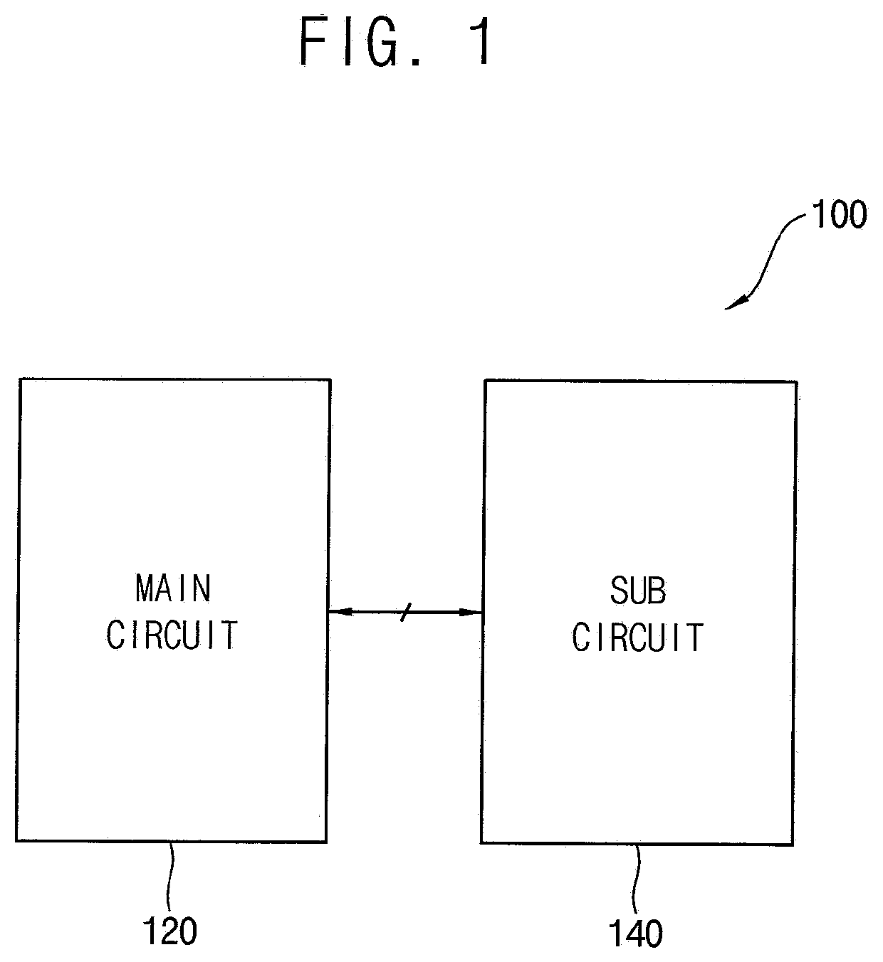
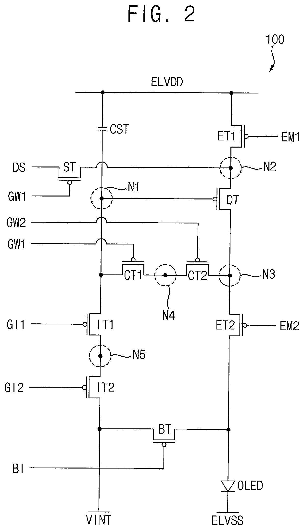
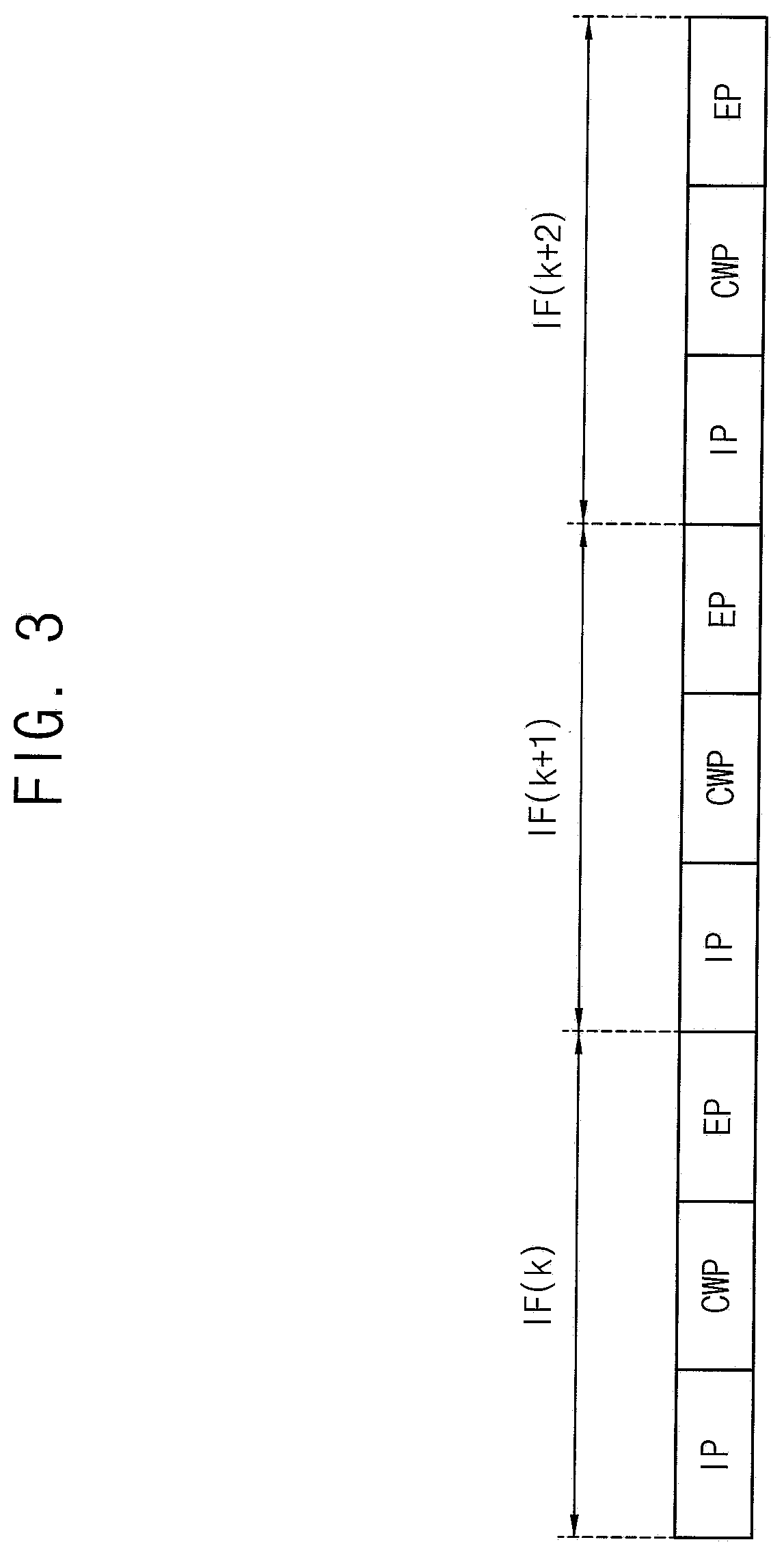
[0051]FIG. 1 is a block diagram illustrating a pixel circuit according to some example embodiments, FIG. 2 is a circuit diagram illustrating an example of the pixel circuit of FIG. 1, and FIG. 3 is a diagram illustrating an example in which the pixel circuit of FIG. 2 operates.

[0052]Referring to FIGS. 1 to 3, the pixel circuit 100 may include a main circuit 120 and a sub circuit 140. For example, as illustrated in FIG. 3, the pixel circuit 100 may sequentially perform a non-light-emitting period (e.g., an initializing period IP and a threshold voltage compensating and data writing period CWP) and a light-emitting period EP in each image frame IF(k), IF(k+1), and IF(k+2). Here, the non-light-emitting period IP+CWP may correspond to a turn-off voltage level period of first and second emission control signals EM1 and EM2, a...


PUM


Abstract

A pixel circuit includes: a main circuit including: a driving transistor that includes a gate terminal connected to a first node, a first terminal connected to a second node, and a second terminal connected to a third node; and an organic light-emitting element connected to the driving transistor and configured to control the organic light-emitting element by controlling a driving current corresponding to a data signal applied via a data line to flow into the organic light-emitting element; and a sub circuit including: a first compensation transistor that includes a gate terminal configured to receive a first gate signal, a first terminal connected to the first node, and a second terminal connected to a fourth node; and a second compensation transistor that includes a gate terminal configured to receive a second gate signal, a first terminal connected to the fourth node, and a second terminal connected to the third node.

Description

CROSS-REFERENCE TO RELATED APPLICATION(S)[0001]The present application claims priority to and the benefit of Korean Patent Application No. 10-2019-0100339, filed on Aug. 16, 2019 in the Korean Intellectual Property Office (KIPO), the contents of which are incorporated herein in its entirety by reference.BACKGROUND1. Field[0002]Aspects of some example embodiments relate generally to a pixel circuit.2. Description of the Related Art[0003]Generally, a pixel circuit included in an organic light-emitting display device may include an organic light-emitting element, a storage capacitor, a switching transistor, a driving transistor, an emission control transistor, a compensation transistor, an initialization transistor, etc. When low temperature poly silicon (LTPS) transistors are utilized in a pixel circuit of an organic light-emitting display device, a flicker may occur when the organic light-emitting display device is driven at less than a specific driving frequency (e.g., at less than ...

Claims


Application Information

Patent Timeline
IPC IPC(8): G09G3/325G09G3/3275
CPCG09G3/325G09G2310/0272G09G3/3275G09G3/3225G09G2320/02G09G3/3233G09G2300/0819G09G2300/0842G09G2300/0861G09G2310/0262G09G2320/0247G09G2340/0435G09G3/3208G09G2300/0439G09G2310/0245
Inventor PARK, SEHYUKGOH, JOON-CHULKWON, SANGANROH, JINYOUNGLEE, HYOJIN
Owner SAMSUNG DISPLAY CO LTD
Why Eureka
Try Eureka