Pressure sensor device

a sensor device and pressure sensor technology, applied in measurement devices, fluid pressure measurement using piezoelectric devices, instruments, etc., can solve the problems of complex structure, difficult to integrate capacitance, and fusion and integration problems, so as to achieve efficient detection

Active Publication Date: 2013-01-22
SEIKO EPSON CORP
View PDF18 Cites 3 Cited by
  • Summary
  • Abstract
  • Description
  • Claims
  • Application Information

AI Technical Summary

Benefits of technology

[0012]According to this aspect of the invention, the change in electric field caused inside the piezoelectric film in response to the piezoelectric film being distorted by the pressure applied to the piezoelectric film can be obtained as an amplified signal of the difference in voltage by the detection circuit (the differential amplifier circuit) for detecting the respective changes in voltages inside the piezoelectric film based on a plurality of piezoelectric capacitances, namely the piezoelectric capacitance between the center electrode and the lower electrode and the piezoelectric capacitance between the peripheral electrode and the lower electrode. Therefore, it is possible to subtract the unnecessary noise included in the change in voltage caused by the distortion of the piezoelectric film and the noise such as the variation of the power supply voltage to balance them out, thus the pressure applied to the piezoelectric film can be detected with high sensitivity without being affected by such noises.
[0014]According to the sensor device, even in the case in which only minute changes occur in voltages inside the piezoelectric film based on the piezoelectric capacitance between the center electrode and the lower electrode and the piezoelectric capacitance between the peripheral electrode and the lower electrode due to the distortion of the piezoelectric film in response to the pressure applied to the piezoelectric film, since the polarity of the charge generated is different between the center electrode and the peripheral electrode, it is possible to increase the differential output voltage. Further, by connecting the differential output electrode composed of the center electrode and the peripheral electrode to the detection circuit having the differential circuit, the pressure sensor device, which has high detection sensitivity, which is not affected by the noises similarly to the case described above, and which is highly sensitive, can be realized.
[0016]According to the sensor device, even in the case in which only minute changes occur in voltages inside the piezoelectric film based on the piezoelectric capacitance between the center electrode and the lower electrode and the piezoelectric capacitance between the peripheral electrode and the lower electrode due to the distortion of the piezoelectric film in response to the pressure applied to the piezoelectric film, since one of the center electrode and the peripheral electrode is disposed in the area where the electric flux density is negative, and the other of the center electrode and the peripheral electrode is disposed in the area where the electric flux density is positive, the polarity of the charge generated is different between the center electrode and the peripheral electrode, and thus the differential output voltage can be increased. Further, by connecting the differential output electrode composed of the center electrode and the peripheral electrode to the detection circuit having the differential circuit, the pressure sensor device, which has high detection sensitivity, which is not affected by the noises similarly to the case described above, and which is highly sensitive, can be realized.
[0018]According to the sensor device, since the voltage level input to the detector such as the differential amplifier circuit can be controlled using the reference voltage Vref, the performance (such as a gain) of the detector can be set to be the optimum value. Therefore, the change in voltage inside the piezoelectric film can be detected, and in particular, with high sensitivity.
[0020]According to the sensor device, since a larger amount of charge is generated at the boundary (boundary between the thick portion and the thin portion) in the periphery of the diaphragm where the compressive stress and the tensile stress are concentrated inside the piezoelectric film in response to the piezoelectric film being distorted due to the pressure applied to the piezoelectric film, the pressure applied to the piezoelectric film can efficiently be detected.

Problems solved by technology

Further, there are still a lot of problems remaining in fusion and integration between MEMS devices and Complementary Metal Oxide Semiconductor (CMOS), and various engineering developments are in progress.
However, since such a capacitance type pressure sensor has low sensitivity, in order for achieving the sensitivity higher than a certain level, the diaphragm 101 needs to have a large area, and at the same time, the structure needs to become complicated.
Therefore, if it is attempted to apply the capacitance type pressure sensor 100 shown in FIG. 15A in the MEMS field, for example, there arises a problem that it is difficult to integrally form the capacitance type pressure sensor and a CMOS circuit or the like, for detecting the pressure applied to the pressure sensor, with each other.
However, in such piezoresistive pressure sensors 110, 120, since it is required to continuously supply the bridge resistors 112 with a constant current flow, there arises a problem that it is not suitable for applications requiring low power consumption.
In particular, since it is required to add another constant current circuit in order for reliably improving the operational accuracy in a high temperature range, there is a problem of incurring a further increase in current consumption.
However, the piezoelectric pressure sensor in the related art has low sensitivity in pressure detection, and has a problem that it is difficult to use the piezoelectric pressure sensor for applications requiring detection of a particularly small pressure variation.

Method used


Image

  • Pressure sensor device
  • Pressure sensor device
  • Pressure sensor device

Examples


embodiment

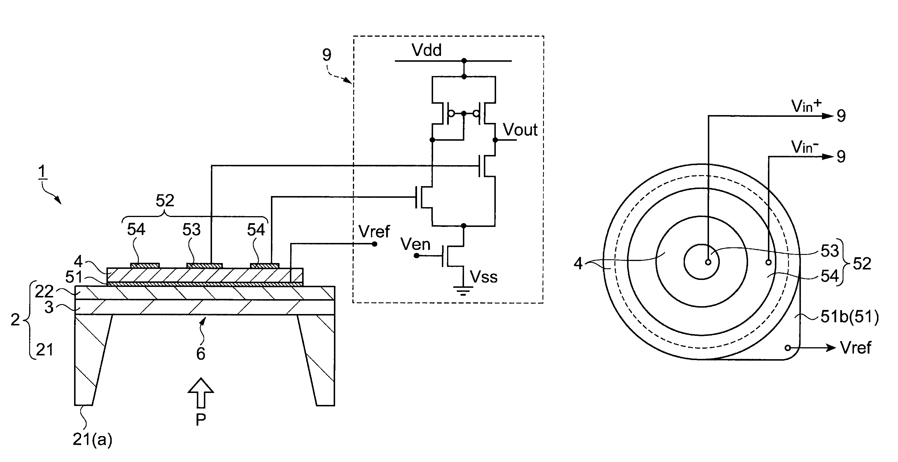
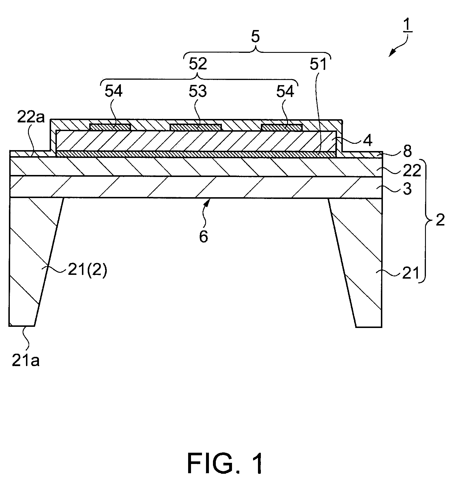
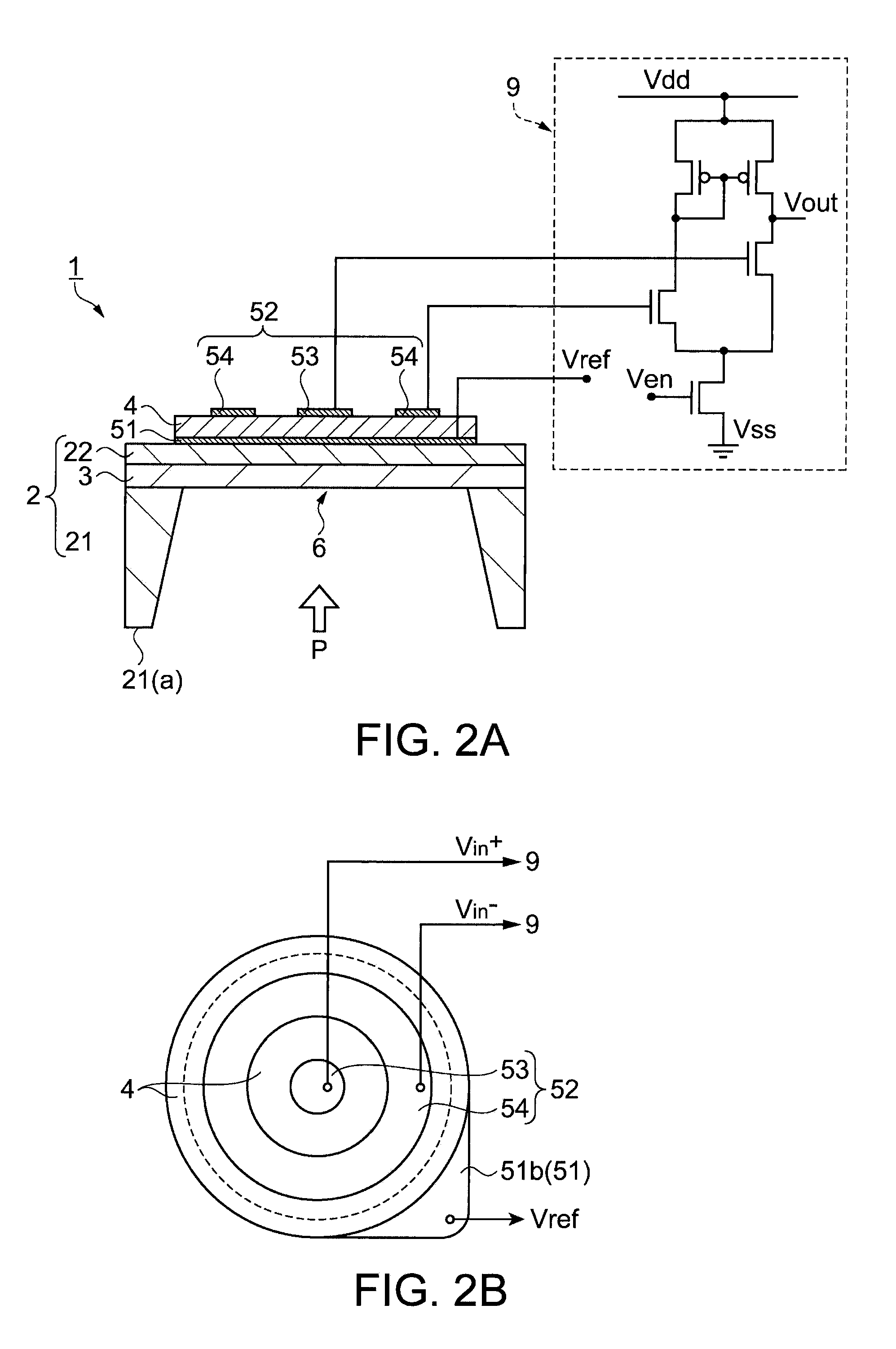
[0042]FIG. 1 is a schematic cross-sectional view showing an example of the pressure sensor device according to the present embodiment. FIGS. 2A and 2B are schematic diagrams showing an example of a semiconductor circuit (a differential amplifier circuit) for detecting the pressure applied to the pressure sensor device. FIG. 3 is a schematic diagram showing an equivalent circuit in the case in which the pressure sensor device and the semiconductor device are connected to each other. FIGS. 4A and 4B are schematic cross-sectional views showing the pressure sensor device according to the present embodiment. FIG. 5 is a schematic cross-sectional view showing another example of the pressure sensor device.

[0043]As shown in FIG. 1, the pressure sensor device 1 is provided with a first substrate 21, a buried oxide film 3 (a buried insulating film), a second substrate 22, a piezoelectric film 4, an electrode 5, and a covering layer 8.

[0044]The buried oxide film 3 is stacked on the first subst...


PUM

PropertyMeasurementUnit
thicknessaaaaaaaaaa
thicknessaaaaaaaaaa
thicknessaaaaaaaaaa

Abstract

A pressure sensor device includes a substrate having a first section and a second section being adjacent to the first section and thinner than the first section, a piezoelectric film having flexibility and disposed on the second section, an upper electrode formed on the piezoelectric film and including a center electrode disposed at a substantially center of the second section in plan view, and a peripheral electrode disposed apart from the center electrode so as to surround the center electrode, a lower electrode formed between the second section and the piezoelectric film and disposed so as to face the upper electrode, and a detection circuit including a differential circuit electrically connected to the center electrode and the peripheral electrode, and the detection circuit detects a difference between a voltage caused between the center electrode and the lower electrode in response to the piezoelectric film being distorted, and a voltage caused between the peripheral electrode and the lower electrode in response to the piezoelectric film being distorted.

Description

BACKGROUND[0001]1. Technical Field[0002]The present invention relates to a pressure sensor device.[0003]2. Related Art[0004]In recent years, integration between Micro Electro Mechanical System (MEMS) and IC has been progressed in the silicon industry, and various types of complex semiconductor devices have been developed. As examples of such devices, in particular, acceleration sensors, gyro sensors, resonators as timing devices, and so on have been developed energetically. Further, there are still a lot of problems remaining in fusion and integration between MEMS devices and Complementary Metal Oxide Semiconductor (CMOS), and various engineering developments are in progress.[0005]In the past, as a pressure sensor for detecting pressure, there have been generally used a capacitance type pressure sensor, a piezoresistive sensor, a piezoelectric sensor, and so on, and in particular, those called a piezoresistive sensor have become mainstream (see e.g., JP-A-7-27643).[0006]Here, as a p...

Claims


Application Information

Patent Timeline
Patent Type & Authority Patents(United States)
IPC IPC(8): G01L9/08
CPCG01L9/008G01L9/08
Inventor TAKIZAWA, TERUO
Owner SEIKO EPSON CORP
Why Eureka
Try Eureka