Electronic device and method for non-contact capacitive and optical pin hole fingerprint detection

a capacitive and optical fingerprint detection technology, applied in the field of electromechanical devices, can solve the problems of insufficient capacitive sensitivity, significant challenges in using the mechanisms involved in fingerprint detection, and inability to achieve capacitive readings, and achieve optimal triggering of optical sensors. , the effect of maximum capacitive readings

Active Publication Date: 2020-02-13
ULTRESFP LLC
View PDF0 Cites 6 Cited by
  • Summary
  • Abstract
  • Description
  • Claims
  • Application Information

AI Technical Summary

Benefits of technology

The patent describes an electronic device with integrated capacitive and optical sensors. The capacitive sensor detects the presence of a finger through a single pin hole opening centered within a ring-shaped electrode. The optical sensor uses a single non-focusing pin hole to capture the peaks and valleys of a fingerprint without touching the device cover. This allows for optimal triggering of the optical sensor when the fingerprint is properly located and in focus above the cover. This integration of sensors reduces manufacturing costs and allows for use in a relatively small and thin electronic device.

Problems solved by technology

If the area stored and later scanned is too small, then verification is insufficient, even though comparison is more readily taken.
Because some portable electronic devices are relatively small, there are significant challenges in using the mechanisms involved in fingerprint detection.
While having a thin overlay increases capacitive sensitivity needed to discern capacitance between fingerprint peaks and valleys, the dimension of the on / off button may be insufficiently small in that not enough of the fingerprint is captured for proper verification.
The cutout is needed since the touch screen display cover is too thick thereby rendering capacitive sensitivity non-feasible.
Requiring a mask layer having a plurality of pin hole openings, each with an overlying and corresponding display pixel, significantly adds to the overall complexity and cost of manufacture.
Even though superior to focusing optical sensors, non-focusing optical sensors and their associated array of pin holes, micro-lenses, and finger contact prove to be less than desirable for fingerprint detection and verification in the slim portable electronic device market.
Thereafter, when the next verification is needed and the next fingerprint is to be detected, the residual left behind on the cover can deleteriously affect the current optical readings.

Method used


Image

  • Electronic device and method for non-contact capacitive and optical pin hole fingerprint detection
  • Electronic device and method for non-contact capacitive and optical pin hole fingerprint detection
  • Electronic device and method for non-contact capacitive and optical pin hole fingerprint detection

Examples


Embodiment Construction

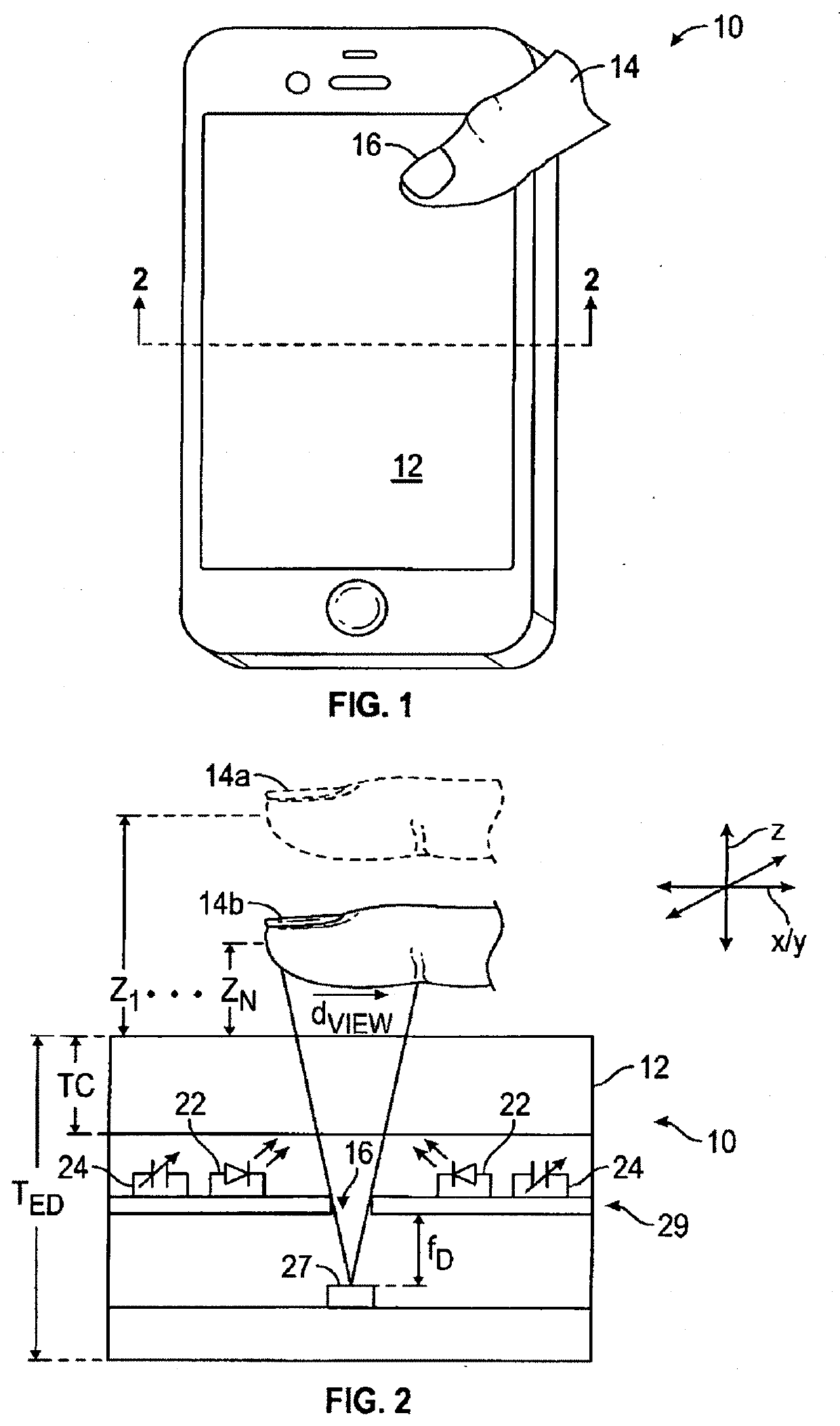
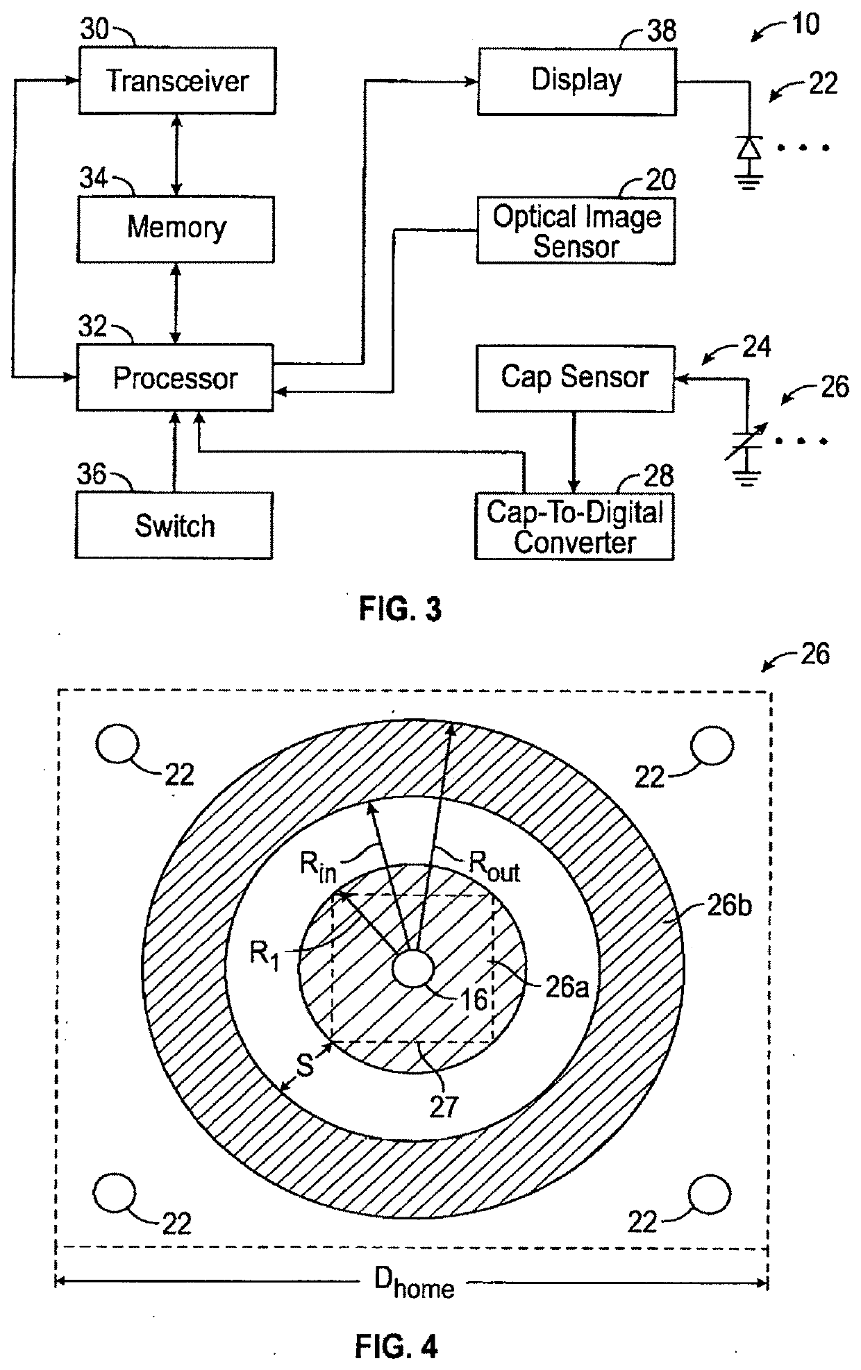
[0037]Turning now to the drawings, FIG. 1 illustrates an electronic device 10. In particular, electronic device 10 is a low profile, relatively small size, preferably portable electronic device. Popular such electronic devices include ones that are relatively slim, and less than, for example, 5-8 mm in thickness. A mobile phone or a tablet are examples of such electronic devices shown having a cover 12 configured over a touch-sensitive display. The display, as well as the cover are on a front-side surface of electronic device 10. The display preferably includes a Graphical User Interface (GUI) that can respond to finger-touch. For example, if the electronic device 10 is a mobile phone, or “smart” phone, there are objects on the display allowing a user to place a cellular call, receive a call, send and receive data, and launch application programs, for example.

[0038]The cover placed over the display is preferably transparent, translucent and / or transmissive to light, both visible and...


PUM


Abstract

An electronic device and method are provided having an optical image sensor and a capacitive proximity sensor. A pin hole opening within a ring electrode of the capacitive proximity sensor is integrated into and used by the optical sensor. Inner and outer electrodes of the ring electrode can be centered about the pin hole opening and spaced apart to perform capacitive proximity detection of a live finger. When brought in proximity to the ring electrode, the finger can be imaged using the present integrated capacitive proximity sensor with an optical sensing mechanism that utilizes the pin hole to not only allow for micro-imaging of an object, such as a finger, but also to provide high resolution fingerprint comparison and blood oxyhemoglobin saturation comparison for biometric control and access to an electronic device, such as a mobile phone.

Description

BACKGROUND1. Field of the Invention[0001]This invention relates to the field of electronic devices and, more particularly, to capacitive and optical fingerprint detection.2. Description of the Relevant Art[0002]The following descriptions and examples are provided as background only, and are intended to reveal information that is believed to be of possible relevance to the present preferred embodiments. No admission is necessarily intended, or should be construed, that any of the following information constitutes prior art impacting the patentable character of the subject matter claimed herein.[0003]Fingerprint detection and matching is a reliable and widely used technique for personal identification or verification. A common approach to fingerprint identification can include scanning a sample fingerprint, or an image thereof, and comparing the scanned fingerprint to a pre-existing stored fingerprint. If the fingerprints match, proper identification of a person can be made to identif...

Claims


Application Information

Patent Timeline
IPC IPC(8): G06K9/00G06F3/041G06F3/044G06V30/144
CPCG06K9/0004G06F3/0412G06F3/044G06K9/00087H04M1/67H04M1/026H04M1/0266H04M2250/12G06V40/1306G06V40/1365G06V40/1318
Inventor AKCASU, OSMAN ERSED
Owner ULTRESFP LLC
Why Eureka
Try Eureka