Thin-film transistor and fabrication method thereof and array substrate

a technology of thin-film transistors and fabrication methods, applied in the field of display technology, can solve the problems of the size of a thin-film transistor, and achieve the effects of improving the electrical performance improving the bending durability of the thin-film transistor, and reducing the area of a pixel

Active Publication Date: 2020-01-16
WUHAN CHINA STAR OPTOELECTRONICS SEMICON DISPLAY TECH CO LTD
View PDF3 Cites 0 Cited by
  • Summary
  • Abstract
  • Description
  • Claims
  • Application Information

AI Technical Summary

Benefits of technology

The present invention relates to a thin-film transistor and its fabrication method, as well as an array substrate that includes the thin-film transistor. The technical effects of this invention include reducing the size and pixel area of the thin-film transistor and improving its electrical performance using a vertical channel design. The invention also simplifies the fabrication process by using a single mask to form the channel layer, gate insulation layer, and gate electrode. The array substrate includes a plurality of the vertical-channel thin-film transistors arranged in an array, which makes the area of a pixel smaller.

Problems solved by technology

Particularly, for high definition flexible mobile phone display screens, virtual reality (VR) display screens, augmented reality (AR) display screens, and holographic display screens that are still under development, the most concerned issue is to reduce the area of a pixel and the size of a thin-film transistor.

Method used


Image

  • Thin-film transistor and fabrication method thereof and array substrate
  • Thin-film transistor and fabrication method thereof and array substrate
  • Thin-film transistor and fabrication method thereof and array substrate

Examples


Embodiment Construction

[0056]To further expound the technical solution adopted in the present invention and the advantages thereof, a detailed description will be given with reference to the preferred embodiments of the present invention and the drawings thereof.

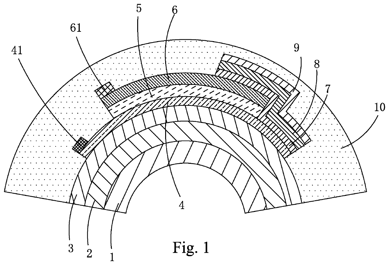
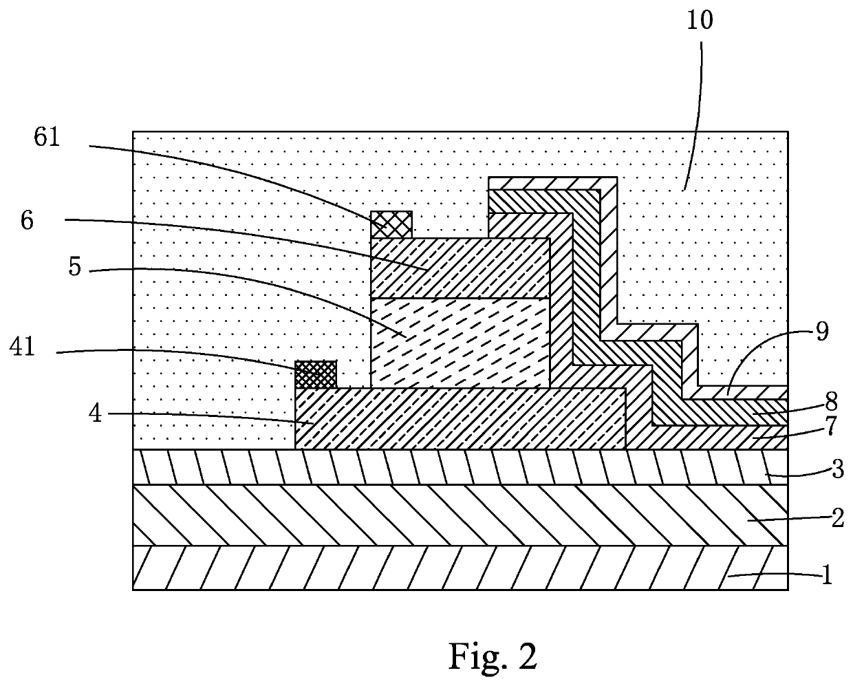
[0057]Referring to both FIGS. 1 and 2, firstly, the present invention provides a thin-film transistor, which comprises:

[0058]a flexible backing 1;

[0059]a moisture / oxygen barrier layer 2 arranged on the flexible backing 1;

[0060]a buffer layer 3 arranged on the moisture / oxygen barrier layer 2;

[0061]a source electrode 4 arranged on the buffer layer 3;

[0062]a separation layer 5 arranged on the source electrode 4 and exposing at least one side portion of the source electrode 4;

[0063]a drain electrode 6 arranged on the separation layer 5;

[0064]an oxide semiconductor channel layer 7 arranged at one side of the separation layer 5 and the drain electrode 6 to sequentially contact a portion of an upper surface of the drain electrode 6, a side surface of the...


PUM


Abstract

The present invention provides a thin-film transistor and a fabrication method thereof, and an array substrate. The thin-film transistor includes a separation layer (5) arranged between the source electrode (4) and the drain electrode (6). An oxide semiconductor channel layer (7) is arranged on one side of the separation layer (5) and the drain electrode (6) to contact a portion of an upper surface of the drain electrode (6), a side surface of the drain electrode (6) and the organic separation layer (5), and a portion of an upper surface of the source electrode (4) to serve as a vertical channel, of which a channel length corresponds to a thickness of the separation layer (5). Varying the thickness of the separation layer to reduce the length of the vertical channel to a sub-micrometer order would greatly reduce the size of the thin-film transistor and reduce the area of a pixel. The vertical channel does not cause a short channel effect so as to improve electrical performance of the thin-film transistor. Using a multiple-layered hexagonal boron nitride film to make a moisture / oxygen barrier layer (2) and using a double-layered graphene film to make the source electrode (4) and the drain electrode (6) help significantly improve bending durability of the thin-film transistor.

Description

CROSS REFERENCE TO RELATED APPLICATION[0001]This is a divisional application of co-pending U.S. patent application Ser. No. 15 / 569,388, filed on Oct. 26, 2017, which is a national stage of PCT Application No. PCT / CN2017 / 101973, filed on Sep. 15, 2017, claiming foreign priority of Chinese Patent Application No. 201710752796.X, filed on Aug. 28, 2017.BACKGROUND OF THE INVENTION1. Field of the Invention[0002]The present invention relates to the field of display technology, and more particular to a thin-film transistor and a fabrication method thereof and an array substrate.2. The Related Arts[0003]In the field of display technology, flat panel displays, such as liquid crystal displays (LCDs) and organic light-emitting diode (OLED) displays, have gradually taken the place of cathode ray tube (CRT) displays.[0004]At present, a mainstream LCD is generally made up of a thin-film transistor (TFT) array substrate and a color filter (CF) substrate that are laminated to each other; and liquid ...

Claims


Application Information

Patent Timeline
Patent Type & Authority Applications(United States)
IPC IPC(8): H01L29/786H01L29/66H01L29/45
CPCH01L21/443H01L29/78603H01L27/1218H01L27/1225H01L29/78642H01L29/78696H01L29/45H01L29/66969H01L29/7869H01L29/0646H01L29/41H01L29/66742H01L29/42384
Inventor BU, CHENGHAO
Owner WUHAN CHINA STAR OPTOELECTRONICS SEMICON DISPLAY TECH CO LTD
Why Eureka
Try Eureka