Semiconductor device

Inactive Publication Date: 2019-11-21
ABLIC INC
View PDF3 Cites 0 Cited by
  • Summary
  • Abstract
  • Description
  • Claims
  • Application Information

AI Technical Summary

Benefits of technology

The present invention relates to a semiconductor device with a Hall element that can accurately remove offset voltage without requiring complicated control circuits. The invention achieves this by using a magnetic sensing portion with a shallow depth and a gentle concentration gradient, which prevents another portion of the semiconductor device from reaching the same depth and being affected by the depletion layer generated from the junction between the magnetic sensing portion and the substrate. This results in accurate removal of the offset voltage without changing the resistance between the electrodes. The invention also reduces the chip size and suppresses the cost by not requiring a depletion layer suppression electrode or a complicated circuit.

Problems solved by technology

It is considered that the offset voltage is generated by imbalance in potential distribution inside the element caused by, for example, mechanical stress applied to the element from the outside or misalignment occurring in a manufacturing process.
However, in case the resistances of the resistors R1, R2, R3, and R4 changes depending on the voltage application direction, the offset voltage cannot be fully removed.
Hence the offset voltage cannot be canceled completely even by the execution of the spinning current method.
Accordingly, there are drawbacks in that the chip size increases, and the cost increases, and so on.

Method used


Image

  • Semiconductor device
  • Semiconductor device
  • Semiconductor device

Examples


Embodiment Construction

[0025]The invention will be now described herein with reference to illustrative embodiments.

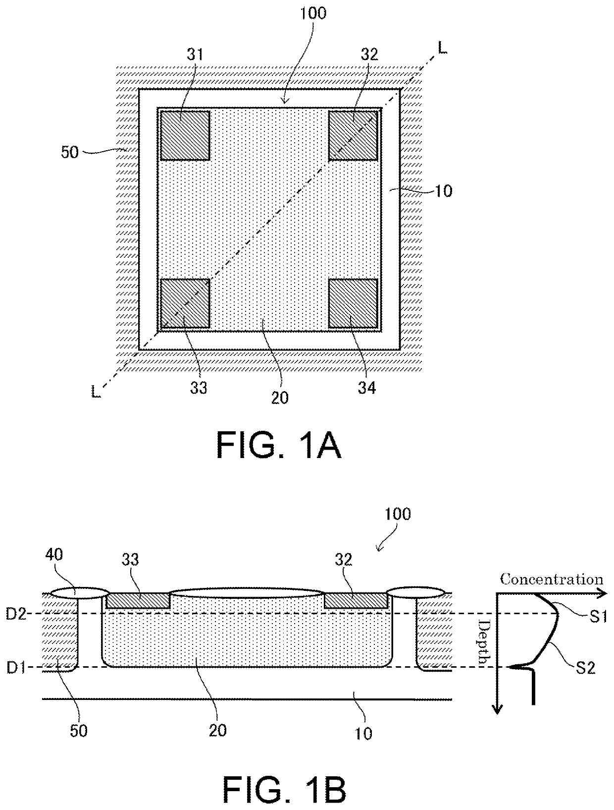
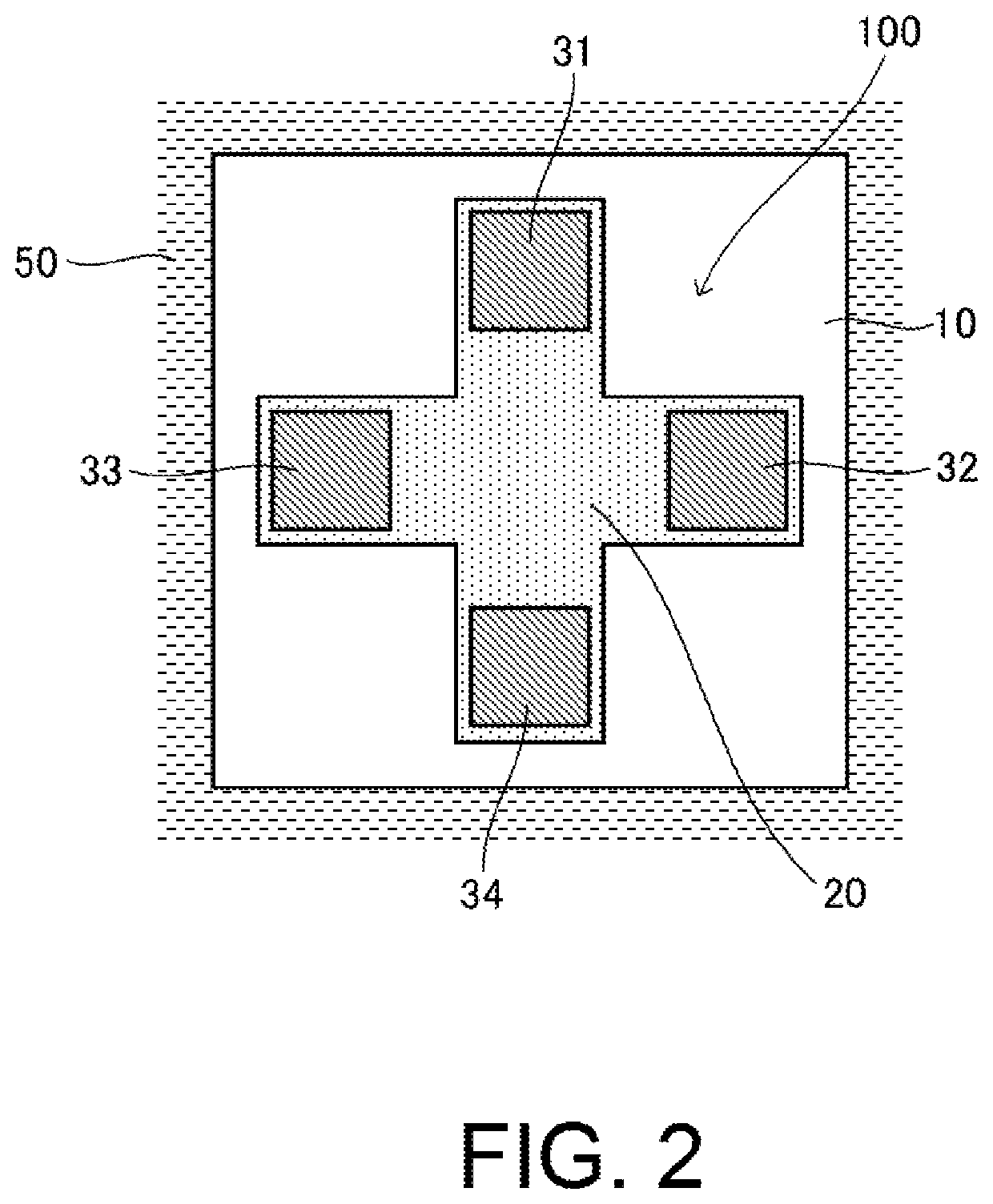
[0026]FIG. 1A and FIG. 1B are views for illustrating a semiconductor device having a Hall element 100 according to one embodiment of the present invention in which FIG. 1A is a plan view, and FIG. 1B is a cross-sectional view taken along the line L-L of FIG. 1A. As illustrated in FIG. 1A and FIG. 1B, the semiconductor device according to the embodiment includes a p-type (first conductivity type) semiconductor substrate 10, the Hall element 100 formed in the semiconductor substrate 10, and a p-type element isolation diffusion layer 50 formed to surround the periphery of the Hall element 100.

[0027]The Hall element 100 is formed of an n-type (second conductivity type) impurity diffusion layer formed in the semiconductor substrate 10, and includes a magnetic sensing portion 20 having a square shape in plan view, and electrodes 31 to 34 which are provided at respective ends in a surface of the mag...


PUM


Abstract

A Hall element includes a magnetic sensing portion formed of an impurity diffusion layer of a second conductivity type, and having four ends, and four electrodes provided at the respective four ends. The impurity diffusion layer forming the magnetic sensing portion has a first depth from a surface of the semiconductor substrate, has a first concentration gradient in which a concentration of impurities of the second conductivity type increases in a depth direction from the surface of the semiconductor substrate to a second depth which is shallower than the first depth, and has a second concentration gradient in which the concentration of the impurities of the second conductivity type decreases in the depth direction from the second depth to the first depth. The second depth is half the first depth or less, and the first concentration gradient is steeper than the second concentration gradient.

Description

RELATED APPLICATIONS[0001]This application claims priority under 35 U.S.C. § 119 to Japanese Patent Application No. 2018-094526 filed on May 16, 2018, the entire content of which is hereby incorporated by reference.BACKGROUND OF THE INVENTION1. Field of the Invention[0002]The present invention relates to a semiconductor device, and more particularly, to a semiconductor device having a Hall element.2. Description of the Related Art[0003]As a magnetic sensor a Hall element is capable of detecting position or angle without contact, and accordingly has various uses.[0004]In an actual Hall element, an output voltage is generated even without an application of magnetic field. The voltage which is an output under a magnetic field of zero is called offset voltage. It is considered that the offset voltage is generated by imbalance in potential distribution inside the element caused by, for example, mechanical stress applied to the element from the outside or misalignment occurring in a manuf...

Claims


Application Information

Patent Timeline
IPC IPC(8): H01L43/06G01R33/07H01L43/04
CPCH01L43/065G01R33/075H01L43/04G01R33/07G01D5/145H10N52/101G01R33/077H10N52/80H10N52/01
Inventor HIOKA, TAKAAKI
Owner ABLIC INC
Why Eureka
Try Eureka