Radio-frequency module and communication apparatus
a radio-frequency module and communication apparatus technology, applied in the direction of printed circuit aspects, cross-talk/noise/interference reduction, association of printed circuit non-printed electric components, etc., can solve the problem of preventing the securement of sufficient ground potential, reducing the distance between wiring lines and electrodes in the module substrate, and generating parasitic inductance and parasitic capacitance, etc. problem, to achieve the effect of suppressing the degradation of radio-frequency transmission characteristic and the radio-frequency transmission characteristic characteristi
- Summary
- Abstract
- Description
- Claims
- Application Information
AI Technical Summary
Benefits of technology
Problems solved by technology
Method used
Image
Examples
first embodiment
[0042][1.1 Configuration of Communication Apparatus]
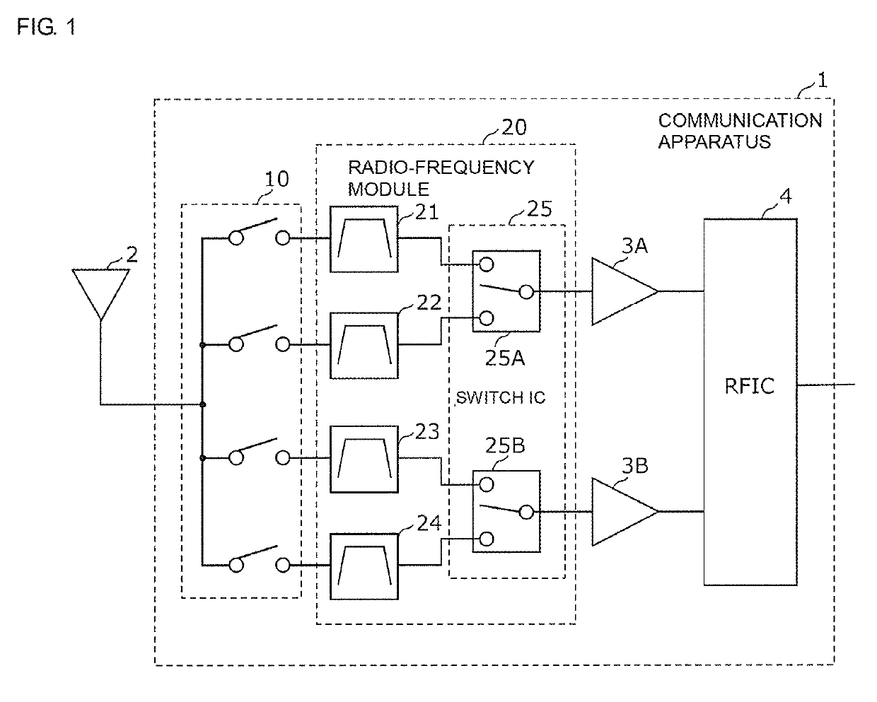
[0043]FIG. 1 is a functional block configuration diagram of a communication apparatus 1 according to a first embodiment. FIG. 1 illustrates the communication apparatus 1 and an antenna element 2. The communication apparatus 1 includes a switch group 10, a radio-frequency (RF) module 20, receiving amplifier circuits 3A and 3B, and an RF signal processing circuit (RFIC) 4. The switch group 10 and the RF module 20 are disposed, for example, at a front-end portion of a multi-mode / multi-band cellular phone.
[0044]The switch group 10 is constituted by one or more switches (in the present embodiment, four SPST switches) each of which connects the antenna element 2 and a signal path corresponding to a predetermined band to each other in response to a control signal from a control unit (not illustrated). The number of signal paths connected to the antenna element 2 at the same time is not limited to one, but may be two or more. In other word...
second embodiment
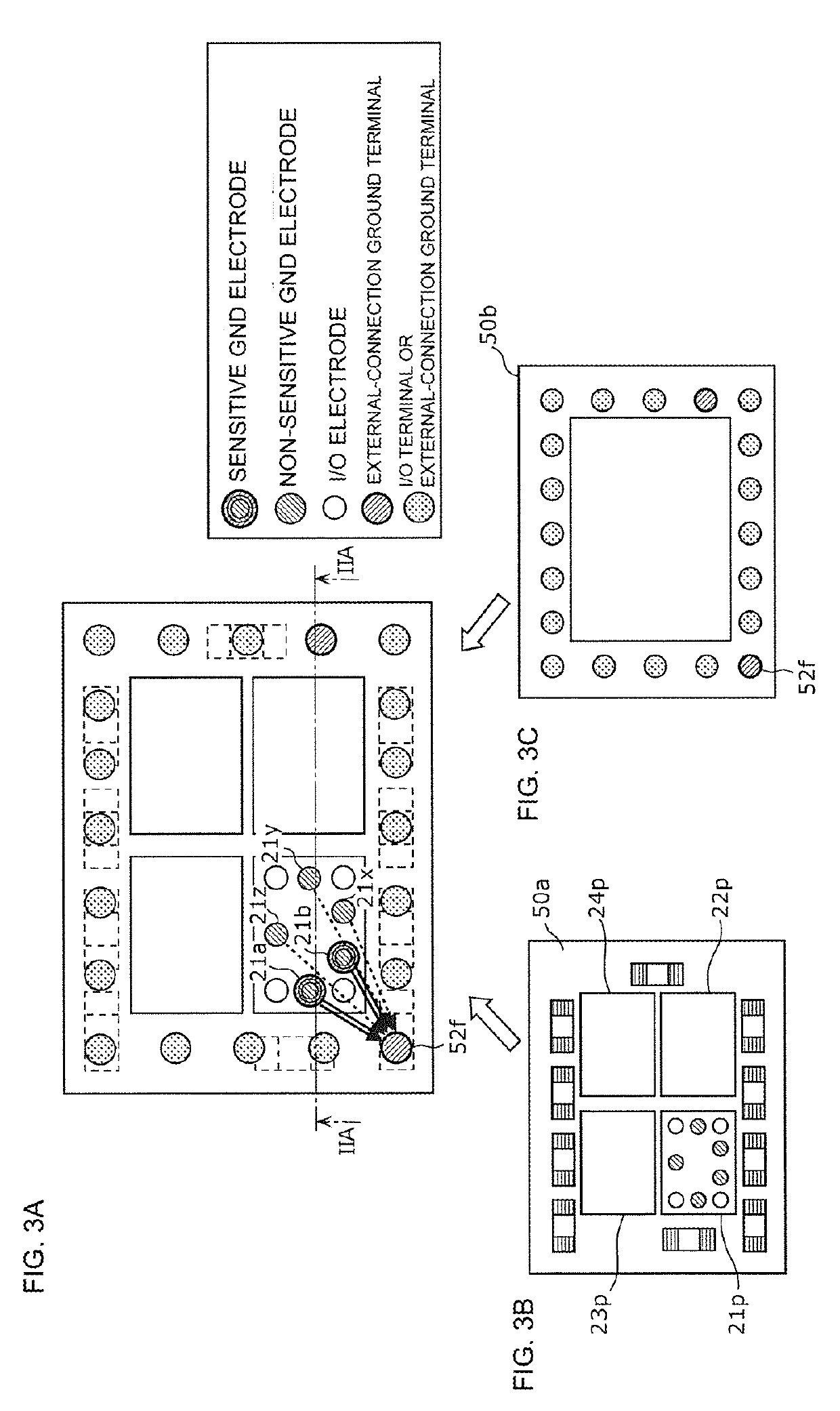
[0107]In the first embodiment, a description has been given of the arrangement of ground electrodes of a filter element mounted on the front surface of a module substrate. In the present embodiment, a description will be given of the arrangement of ground electrodes of an IC chip mounted on a module substrate.
[2.1 Configuration of RF Module]
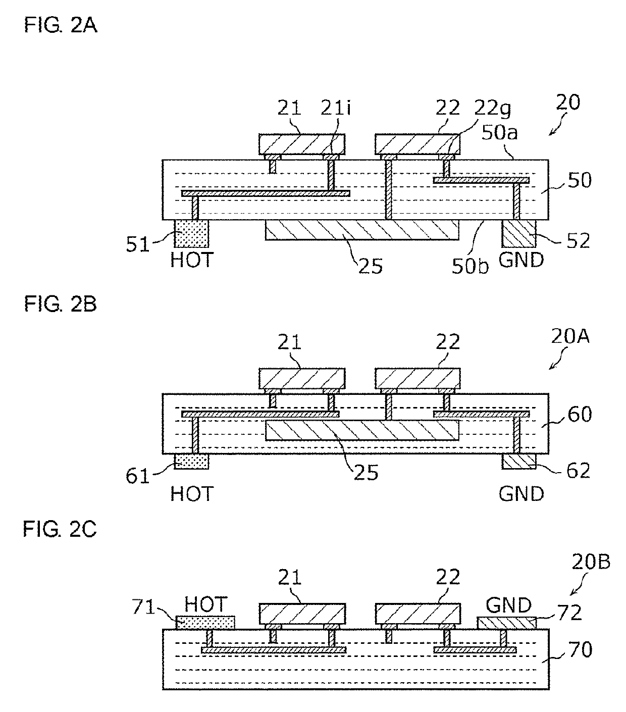
[0108]FIG. 7 is a plan view illustrating the arrangement relationship among electrodes and terminals of the RF module according to the second embodiment. The RF module according to the present embodiment has the cross-sectional configuration illustrated in FIG. 2A. FIG. 7 is a perspective plan view illustrating the arrangement and connection relationships among the individual terminals disposed in an outer peripheral portion of the rear surface of the module substrate 50 and the individual electrodes disposed (in a partial region) in the switch IC 25.
[0109]FIG. 7 illustrates external-connection ground terminals 52b, 52d, and 52e and a plurality o...
PUM
 Abstract
Description
Claims
Application Information
 - R&D
- Intellectual Property
- Life Sciences
- Materials
- Tech Scout
- Unparalleled Data Quality
- Higher Quality Content
- 60% Fewer Hallucinations
Browse by: Latest US Patents, China's latest patents, Technical Efficacy Thesaurus, Application Domain, Technology Topic, Popular Technical Reports.
© 2025 PatSnap. All rights reserved.Legal|Privacy policy|Modern Slavery Act Transparency Statement|Sitemap|About US| Contact US: help@patsnap.com


