
Semiconductor device and test method

a technology of semiconductors and test methods, applied in the direction of pulse automatic control, pulse characteristics measurement, instruments, etc., can solve the problems of deterioration of the properties of the correction circuit during normal operation, difficulty in testing, and the above mentioned phase difference voltage error, etc., and achieve the effect of easy product shipmen

Active Publication Date: 2019-06-27
LAPIS SEMICON CO LTD
View PDF0 Cites 0 Cited by
  • Summary
  • Abstract
  • Description
  • Claims
  • Application Information

AI Technical Summary

Benefits of technology

The present invention provides a semiconductor device and a test method that allow for easy testing before product shipment without affecting the device's normal operation. This method uses a less expensive tester and eliminates the need for a switch element to output the correction current, reducing the possibility of parasitic capacitance or leakage paths. Overall, this invention enables efficient and reliable testing of the correction circuit before shipment.

Problems solved by technology

Those PLL circuits mentioned above may be subjected to an error in the phase difference voltage, which is produced by the charge pump, due to variations during manufacture.
However, to measure the current value of the correction current, it is necessary to measure the current with high accuracy, thus causing the test to be made with difficulty.
In addition, since the aforementioned switch and external terminal are connected to the output end of the correction circuit, there was a possibility of deterioration in the properties of the correction circuit during normal operation due to the parasitic capacitance or leakage path of the switch.

Method used


Image

  • Semiconductor device and test method
  • Semiconductor device and test method
  • Semiconductor device and test method

Examples


Embodiment Construction

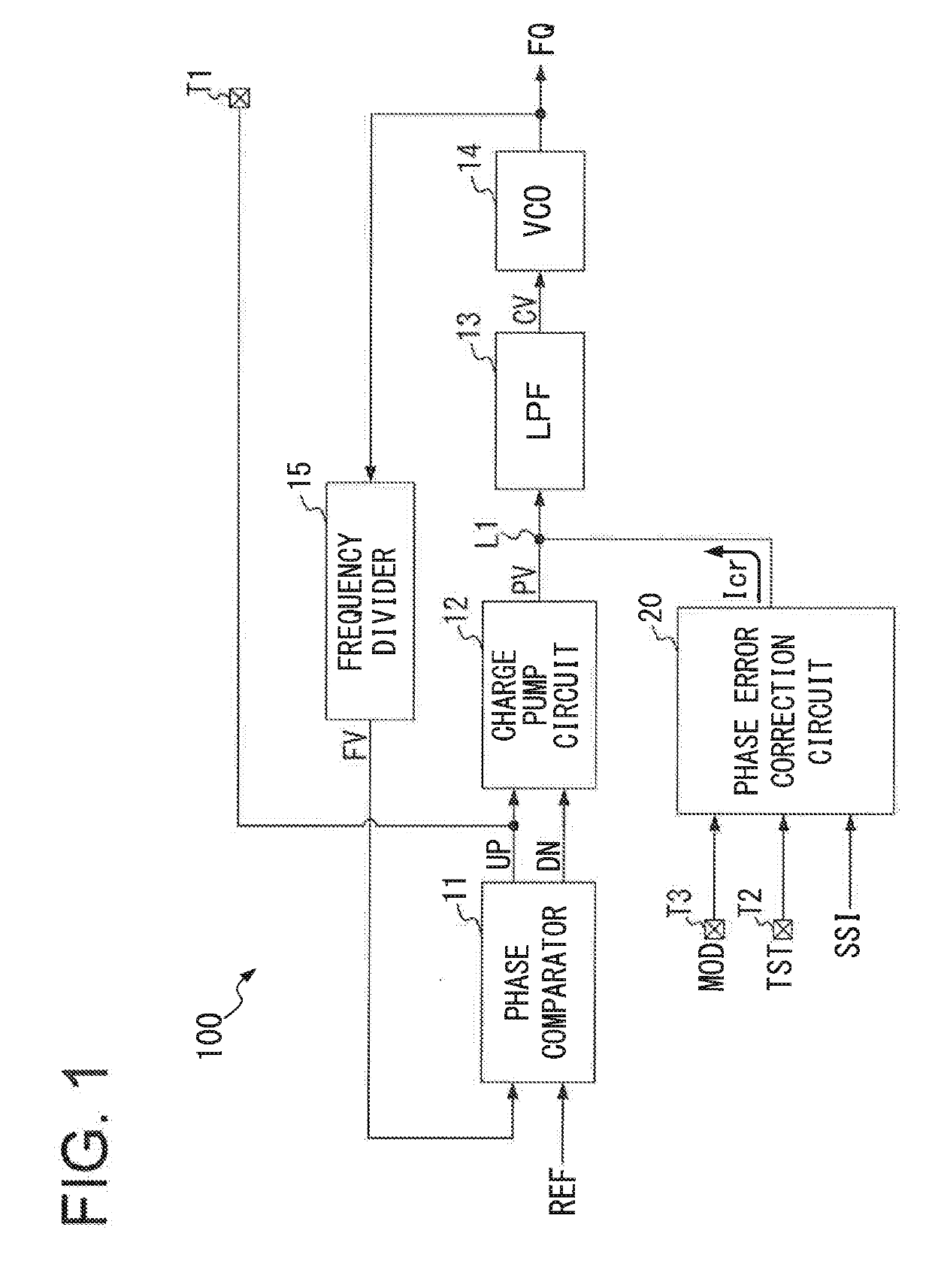
[0020]FIG. 1 is a block diagram illustrating a configuration of a PLL (Phase-Locked Loop) circuit 100 included in a semiconductor IC (Integrated Circuit) chip serving as a semiconductor device according to the present invention.

[0021]The PLL circuit 100 produces an oscillation signal FQ in phase synchronism with an entered reference signal REF. Note that the PLL circuit 100 includes a so-called spectrum diffusion function for adding jitter to the oscillation signal FQ in order to prevent energy from concentrating on a particular frequency.

[0022]The PLL circuit 100 includes a phase comparator 11, a charge pump circuit 12, a loop filter (LPF) 13, a VCO (Voltage-controlled oscillator) 14, a frequency divider 15, and a phase error correction circuit 20.

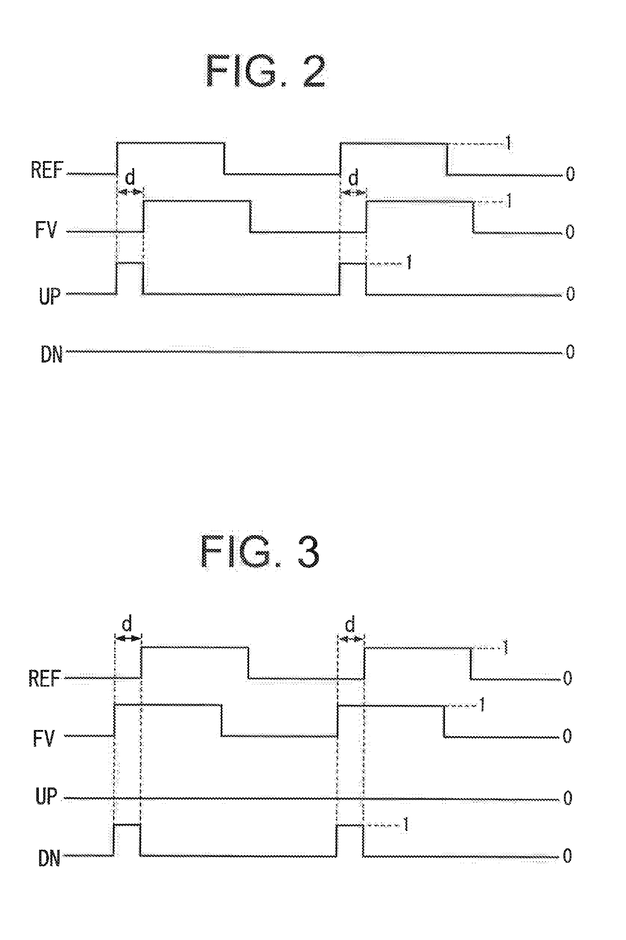
[0023]The phase comparator 11 detects the phase difference between the rising edge of the reference signal REF having a predetermined frequency and the rising edge of a divided oscillation signal FV supplied from the frequency divider 15....


PUM


Abstract

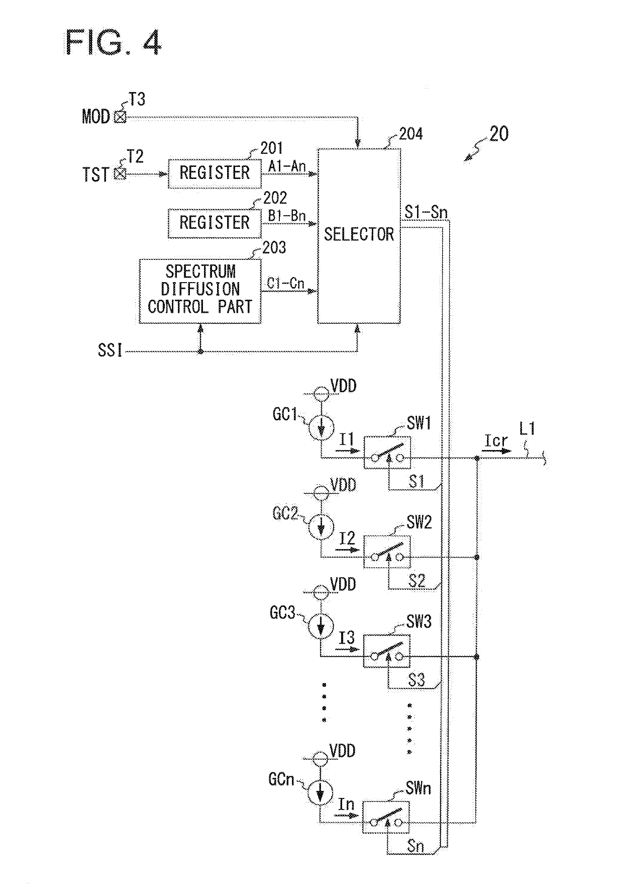
A semiconductor device according to the present invention has a PLL circuit which includes: a phase comparison part that detects the phase difference between a reference signal and an oscillation signal to produce a phase difference signal indicative of the phase difference in binary and then output the produces signal to outside through a first external terminal; a voltage conversion part that applies, to a phase difference voltage node, a phase difference voltage having a voltage value corresponding to the phase difference represented by the phase difference signal; an oscillation part that produces, as an oscillation signal, a signal having a frequency depending on the phase difference voltage; and a correction circuit that supplies a correction current to the phase difference voltage node, and upon reception of a test control signal at a second external terminal, supplies a current depending on the test control signal to the phase difference voltage node as a correction current.

Description

BACKGROUND1. Technical Field[0001]The present invention relates to semiconductor devices, and more particularly, to a semiconductor device which includes a PLL (Phase-Locked Loop) circuit, and a method for testing the semiconductor device.2. Description of the Related Art[0002]A digital PLL circuit is known as a PLL circuit, wherein such a digital PLL circuit includes: a phase comparator configured to produce a phase difference signal indicative of the phase difference in binary between a reference signal and an oscillation signal; and a charge pump configured to supply a current depending on the phase difference signal to a node, thereby producing a phase difference voltage corresponding to the phase difference signal at the node.[0003]On the other hand, a technique has been suggested for such a digital PLL circuit, wherein the technique adjusts, depending on the magnitude of the phase difference mentioned above, the amount of current to be produced by the charge pump (for example,...

Claims


Application Information

Patent Timeline
Patent Type & Authority Applications(United States)
IPC IPC(8): H03L7/089G01R29/02G01R31/26
CPCH03L7/0895G01R29/023G01R31/2607H03L7/089G01R31/31725H03L7/085
Inventor YAGI, KATSUYOSHI
Owner LAPIS SEMICON CO LTD
Learn More