Silicon carbide mosfet inverter circuit

Active Publication Date: 2019-04-18
FUJI ELECTRIC CO LTD
View PDF0 Cites 1 Cited by
  • Summary
  • Abstract
  • Description
  • Claims
  • Application Information

AI Technical Summary

Benefits of technology

The present invention aims to provide a silicon carbide MOSFET inverter circuit that can suppress the expansion of stacking faults during deadtime. This is achieved by shortening the pulse width of transient current flowing to the built-in diodes during deadtime, which makes it possible to prevent degradation of the inverter circuit's characteristics and to improve its reliability.

Problems solved by technology

Transient current flows to the built-in diodes 26, 27 during this deadtime, thus causing stacking faults to grow.

Method used


Image

  • Silicon carbide mosfet inverter circuit
  • Silicon carbide mosfet inverter circuit
  • Silicon carbide mosfet inverter circuit

Examples


embodiment

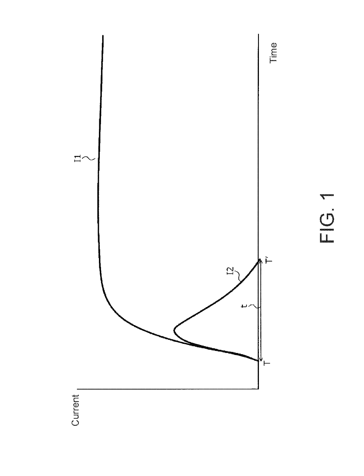
[0042]The configuration of the silicon carbide MOSFET of this embodiment is similar to the configuration of a conventional silicon carbide semiconductor device, and thus a disclosure and description thereof will be omitted. The conventional silicon carbide semiconductor device described in FIG. 5 was a planar structure silicon carbide MOSFET in which the channel is formed parallel to the substrate surface, but the present invention can be applied to a vertical MOSFET having a trench structure in which the channel is formed in a direction perpendicular to the substrate surface, for example. The present invention can be applied to a silicon carbide MOSFET used in an inverter circuit.

[0043]Furthermore, the configuration of the silicon carbide MOSFET inverter circuit of this embodiment is similar to the configuration of a conventional silicon carbide MOSFET inverter circuit (shown in FIG. 6), and thus a disclosure thereof will be omitted. In the silicon carbide MOSFET inverter circuit o...


PUM


Abstract

The inverter circuit has a first silicon carbide MOSFET and a second silicon carbide MOSFET connected in series and external freewheel diodes respectively connected in anti-parallel to the first and second MOSFETs. The inverter circuit is configured such that during a deadtime when the first silicon carbide MOSFET and the second silicon carbide MOSFET are OFF and freewheeling current starts flowing, a pulse width of a transient current flowing to a built-in diode of the first silicon carbide MOSFET or a built-in diode of the second silicon carbide MOSFET is less than 2 μs.

Description

BACKGROUND OF THE INVENTIONTechnical Field[0001]This invention relates to a silicon carbide MOSFET inverter circuit.Background Art[0002]Silicon (Si) is conventionally used as the constituting material for power semiconductor devices, which control high voltages and large currents. There are several types of power semiconductor devices, such as bipolar transistors or IGBTs (insulated gate bipolar transistors) and MOSFETs (metal oxide semiconductor field effect transistors), each specialized for different uses.[0003]For example, bipolar transistors or IGBTs have higher current density than MOSFETs and can have large currents, but cannot be switched at high speeds. Specifically, bipolar transistors are limited to switching frequencies of approximately several kHz, and IGBTs are limited to switching frequencies of approximately several dozen kHz. On the other hand, power MOSFETs have lower current density than bipolar transistors or IGBTs and cannot easily have large currents, but can h...

Claims


Application Information

Patent Timeline
IPC IPC(8): H02M7/537H01L29/16H01L27/06H02M1/38
CPCH02M7/537H01L29/1608H01L27/0629H02M1/38H02M7/5395H01L29/7802H01L29/1095Y02B70/10H02M1/0054H02M1/385
Inventor FUJIMOTO, TAKUMICHOUNABAYASHI, MIKIYA
Owner FUJI ELECTRIC CO LTD
Why Eureka
Try Eureka