Two-dimensional electronic devices and related fabrication methods

a technology of electronic devices and fabrication methods, applied in the direction of semiconductor devices, basic electric elements, electrical equipment, etc., can solve the problems of large material interface damage, significant stoichiometric non-uniformity in films, structure imperfections, etc., to achieve perfect stoichiometric uniformity, good uniformity and conformity, and accurate atomic-scale thickness controllability

Inactive Publication Date: 2018-10-25
CHANG YU CHEN
View PDF14 Cites 6 Cited by
  • Summary
  • Abstract
  • Description
  • Claims
  • Application Information

AI Technical Summary

Benefits of technology

[0006]As an alternative deposition method, atomic layer deposition (ALD) method which enables layer-by-layer growth of high-quality films through self-limiting surface reactions is considered. The ALD method has numerous advantages over other thin-film techniques, such as, for example, good uniformity and conformality, accurate atomic-scale thickness controllability, perfect stoichiometric uniformity, low impurity contamination, and low deposition temperature (below 400° C.) which enables the utilization of temperature sensitive substrates, for example, biological materials and polymers that could be destroyed or compromised at conventional process temperature.
[0007]Moreover, the ALD method has strong capabilities to control the optoelectronic characteristics of the ALD-derived semiconductor thin films, including Hall carrier mobility, electrical resistivity, electrical conductivity, light transparency, and photon-electron conversion efficiency. Therefore, ALD fabricating technique can be advantageous in depositing two-dimensional semiconductor films with greater control over layer optoelectronic properties.

Problems solved by technology

However, these high energy methods typically result in broad material interface damage, significant stoichiometric non-uniformity in films, and structure imperfections such as, for example, micro pinholes and point-defects.
However, the problems relating to efficient doping and controlling the optoelectronic properties of the films have remained as technological issues to be solved.
With the continual trend towards scaling down modern electronic devices to micro- and nano-levels, such issues may become even more severe and can degrade the material quality tremendously.

Method used


Image

  • Two-dimensional electronic devices and related fabrication methods
  • Two-dimensional electronic devices and related fabrication methods
  • Two-dimensional electronic devices and related fabrication methods

Examples


Embodiment Construction

[0038]Reference will now be made in detail to exemplary embodiments consistent with the present invention, examples of which are illustrated in the accompanying drawings. Wherever possible, the same reference numbers will be used throughout the drawings to refer to the same or like parts.

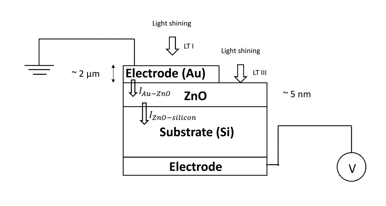
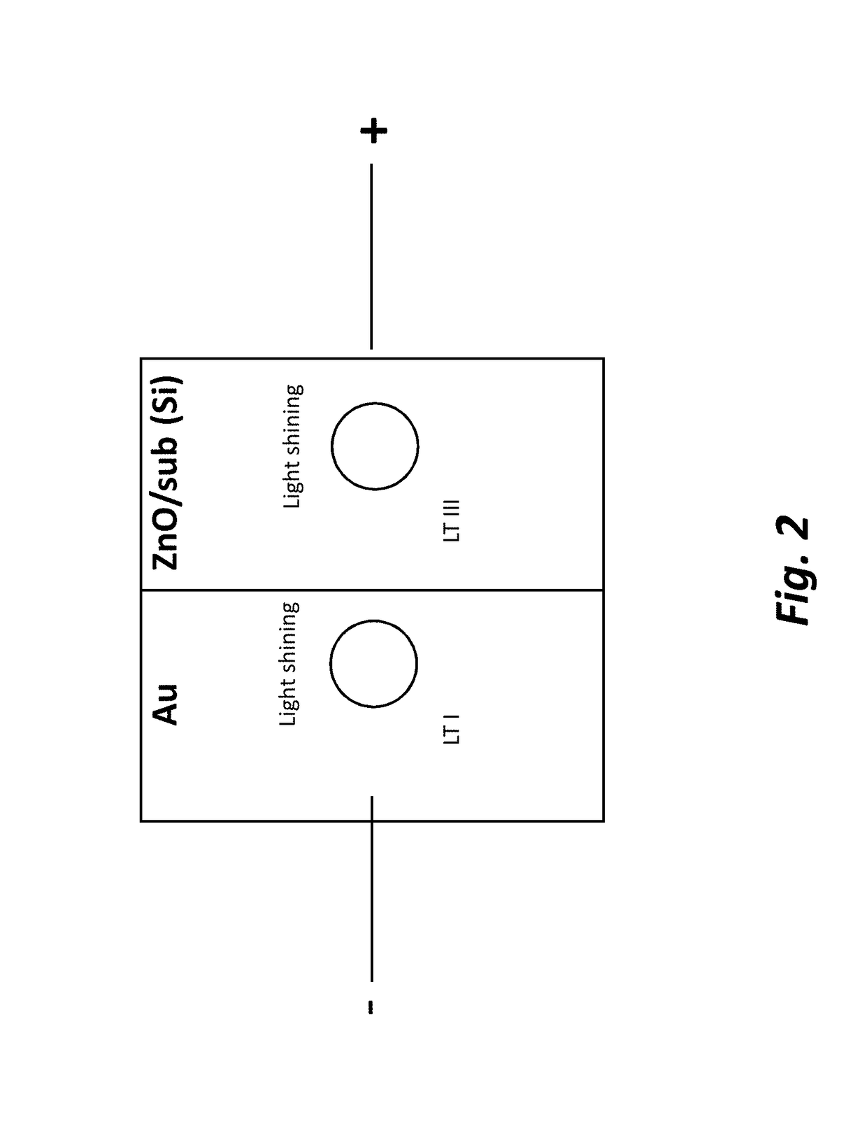
[0039]Photodetectors (PD) are one of the basic building blocks of an optoelectronic link, where it performs optical-to-electrical signal conversion. Development of Si-based PDs (Si-PDs) for telecommunication wavelengths (1.3-1.6 μm) based on the mature CMOS technology is an essential step for monolithic, on-chip, optoelectronic integration. While Si-PDs are widely employed in the visible spectral range (0.4-0.7 μm), they are not suitable for detecting near-infrared (NIR) radiation above 1.1 μm because the energy of NIR photons at telecommunication wavelengths (0.78-0.95 eV) is not sufficient to overcome the Si bandgap (indirect, 1.12 eV) and induces photogeneration of electron-hole pairs (i.e., no p...


PUM


Abstract

Various embodiments of a semiconductor device and related fabrication methods are disclosed. In one exemplary embodiment, the semiconductor device may include a substrate and a plurality of two-dimensional semiconductor films over the substrate, where a photogain of the two-dimensional films is above about 103 when measured at room temperature. In another exemplary embodiment, a semiconductor device may comprise a substrate comprising nanorods or nanodots and a plurality of two-dimensional films disposed on the substrate.

Description

FIELD OF THE INVENTION[0001]Various embodiments of the present disclosure relate generally to two-dimensional electronic devices and related fabrication methods. More specifically, particular embodiments of the present disclosure relate to group II-VI semiconductor films with high optoelectronic conversion efficiency and methods of depositing group II-VI semiconductor films on a semiconductor device.DESCRIPTION OF RELATED ART[0002]Two-dimensional, group II-VI semiconductor films have become a field of increasing technological interest due to their unique properties and their potential applications in various types of optoelectronic devices, such as ultraviolet emission devices, light emitting diodes, laser diodes, solar cells, surface acoustic wave devices, photon detectors, transparent conductive films, waveguides, gas pressure sensors, microsensors, interfacial coatings for fiber strength enhancement, invisible thin film transistors, field emitters, field effect transistors, and p...

Claims


Application Information

Patent Timeline
Patent Type & Authority Applications(United States)
IPC IPC(8): H01L29/227H01L21/02H01L31/0296
CPCH01L29/227H01L21/02554H01L31/02963H01L31/035227H01L31/074H01L31/109H01L31/18Y02E10/50
Inventor CHANG, YU-CHEN
Owner CHANG YU CHEN
Why Eureka
Try Eureka