Method for preparing semiconductor nanocrystal siloxane composite resin composition

Active Publication Date: 2018-09-27
KOREA ADVANCED INST OF SCI & TECH
View PDF0 Cites 0 Cited by
  • Summary
  • Abstract
  • Description
  • Claims
  • Application Information

AI Technical Summary

Benefits of technology

The present invention is a method for preparing a resin composition containing semiconductor nanocrystals. The method allows for uniform dispersion and encapsulation of the nanocrystals in the resin through chemical interaction and bonding, without the need for an organic ligand exchange. The resulting cured product has high reliability and quantum efficiency, protecting the nanocrystals from external oxidizing environments. In a moisture oxidizing environment, the quantum efficiency of the nanocrystals is increased, further enhancing the reliability of devices utilizing the resin composition and cured products. The method can be applied in fields of optics and displays.

Problems solved by technology

However, when the semiconductor nanocrystals are flaked in a polymer resin, the high surface energy of the semiconductor nanocrystals and incompatibility between organic hydrocarbon based ligand of semiconductor nanocrystals and polymer matrix cause the aggregation of semiconductor nanocrystals.
Accordingly, a process for ligand exchange of the semiconductor nanocrystals which imparts the compatibility with the polymer resin is essentially needed, and also, artificially flaked semiconductor nanocrystals polymer resins are weak in long-term storage stability.
In addition, in order to practically apply the semiconductor nanocrystals to optical devices, reliability that maintains optical characteristics (quantum efficiency) of the semiconductor nanocrystals without deterioration must be ensured, but the semiconductor nanocrystals composed of metals are easily oxidized in an oxidizing environment of heat, oxygen, and moisture, which causes serious deterioration in the quantum efficiency of the semiconductor nanocrystals.
However, the methods for exchanging the organic ligand of the semiconductor nanocrystal proposed above have the following problems.
In this case, defects inevitably occur on the surface of the semiconductor nanocrystals, and this is accompanied by a serious reduction in quantum efficiency, which is an inherent optical characteristic of the semiconductor nanocrystals.

Method used


Image

  • Method for preparing semiconductor nanocrystal siloxane composite resin composition
  • Method for preparing semiconductor nanocrystal siloxane composite resin composition
  • Method for preparing semiconductor nanocrystal siloxane composite resin composition

Examples


example 1

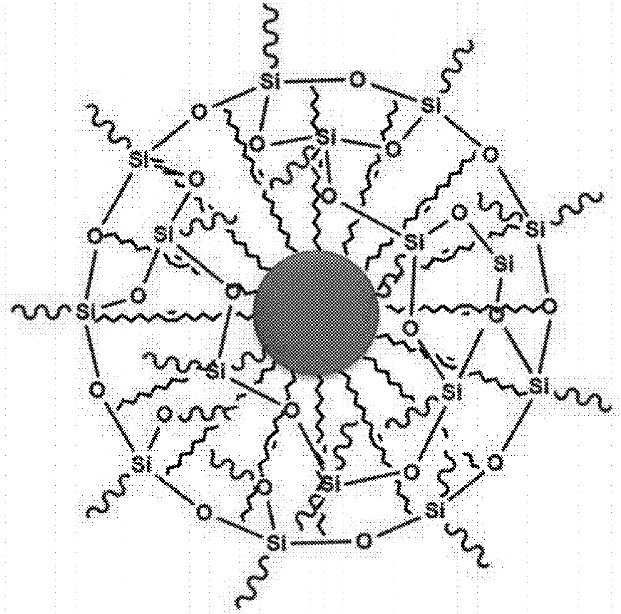
[0131]3-(meth)acryloxypropyltrimethoxysilane and diphenylsilanediol were added to a 250 ml 2-neck flask at a molar ratio of 1:1, and then barium hydroxide monohydrate (Ba(OH)2.H2O) was added as a catalyst in an amount of 0.1 mol % relative to silane.

[0132]Then, the mixture was stirred at 85° C. for 5 hours to perform a non-hydrolytic condensation reaction.

[0133]At this time, semiconductor nanocrystals were added as a mixture during stirring of organosilane mixture so that the semiconductor nanocrystals were dispersed during the formation of a siloxane structure, thereby preparing a siloxane composite resin composition.

[0134]As for the semiconductor nanocrystals used above, Nanodot-HE-620 (trade name, Ecoflux, Korea) having a Cd-based core-shell structure was used.

[0135]The semiconductor nanocrystals were dispersed in a chloroform solvent, and added in an amount of 1.0 parts by weight based on 100 parts by weight of the siloxane resin (excluding the weight of the solvent).

[0136]When ...

example 2

[0138]A semiconductor nanocrystal siloxane composite resin composition was prepared in the same manner as in Example 1, except that 3-(meth)acryloxypropyltrimethoxysilane and diisobutylsilanediol were used at a molar ratio of 1:1 instead of 3-(meth)acryloxypropyltrimethoxysilane and diphenylsilanediol and that sodium hydroxide was added as a catalyst in an amount of 0.1 mol % relative to silane.

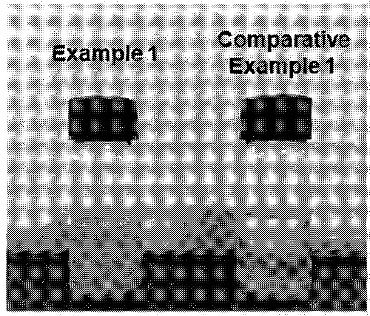
[0139]The semiconductor nanocrystal siloxane composite resin composition thus prepared was placed into a circular mold having a diameter of 1 cm and molded to a thickness of 1 mm, and then exposed to an ultraviolet lamp of a wavelength of 365 nm for 10 minutes to prepare a cured product.

example 3

[0140]A semiconductor nanocrystal siloxane composite resin composition was prepared in the same manner as in Example 1, except that 3-(meth)acryloxypropyltrimethoxysilane and 1,4-bis(hydroxydimethylsilyl)benzene were used at a molar ratio of 1:1 instead of 3-(meth)acryloxypropyltrimethoxysilane and diphenylsilanediol and that tetraalkylammonium hydroxide was added as a catalyst in an amount of 0.1 mol % relative to silane.

[0141]The semiconductor nanocrystal siloxane composite resin composition thus prepared was placed into a circular mold having a diameter of 1 cm and molded to a thickness of 1 mm, and then exposed to an ultraviolet lamp of a wavelength of 365 nm for 10 minutes to prepare a cured product.


PUM

PropertyMeasurementUnit
Percent by massaaaaaaaaaa
Weightaaaaaaaaaa

Abstract

The present invention relates to a method for preparing a semiconductor nanocrystal siloxane composite resin composition, and a cured product using the same. In the preparation method, the semiconductor nanocrystals are added during a non-hydrolytic sol-gel condensation reaction for forming a siloxane structure so that a siloxane resin having a dense inorganic network, which includes a siloxane bond, is encapsulated and thus is dispersed in the semiconductor nanocrystals through a chemical interaction and a chemical bond, thereby preventing a reduction in inherent characteristics (quantum efficiency) of the semiconductor nanocrystals resulting from an external oxidizing environment. Accordingly, when the curing of the resin composition is carried out, a cured product, which can be applied to various applications including a semiconductor nanocrystal siloxane composite having excellent reliability, can be provided.

Description

TECHNICAL FIELD[0001]This application claims priority to and the benefit of Korean Patent Application No. 10-2017-0037832 filed on Mar. 24, 2017 with the Korean Intellectual Property Office, the disclosure of which is incorporated herein by reference in its entirety.[0002]The present invention relates to a method for preparing a semiconductor nanocrystal siloxane composite resin composition, and a cured product using the resin composition obtained therefrom.BACKGROUND ART[0003]Semiconductor nanocrystals, which are widely known as quantum dots, have a very small size in the range of several nanometers. Thus, the semiconductor nanocrystals exhibit different optical and physical properties from those inherent to bulk semiconductors due to the quantum confinement effect.[0004]As the energy bandgap varies according to a change in size of the semiconductor nanocrystals due to the quantum confinement effect, the semiconductor nanocrystals may exhibit different optical and physical properti...

Claims


Application Information

Patent Timeline
IPC IPC(8): C09K11/02C08G77/52C09K11/54H01L33/50H01L33/56C09K11/70C09K11/88C09K11/56
CPCC09K11/02C08G77/52C09K11/54H01L33/502H01L33/56C09K11/703C09K11/883C09K11/565C08G77/80C08G77/70H01L2933/0033H01L2933/0041H01L2933/005C08G77/20C08L83/04C08K3/08C08K5/07C08K3/013C08G77/08C08G77/18C08K9/02C08G2190/00C08L2203/20C08L2203/16C08K2201/011H01B1/08
Inventor BAE, BYEONG-SOOKIM, HWEA YOONJANG, JUNHO
Owner KOREA ADVANCED INST OF SCI & TECH
Why Eureka
Try Eureka