Insoles for Insertion into an Article of Footwear and System for Monitoring a Foot Pressure
a technology for foot pressure and insoles, applied in the field of foot pressure monitoring, can solve the problems of insoles suffering strong stress and structural constraints, preventing an easy integration in various footwear articles, and malfunctioning insoles
- Summary
- Abstract
- Description
- Claims
- Application Information
AI Technical Summary
Benefits of technology
Problems solved by technology
Method used
Image
Examples
first embodiment
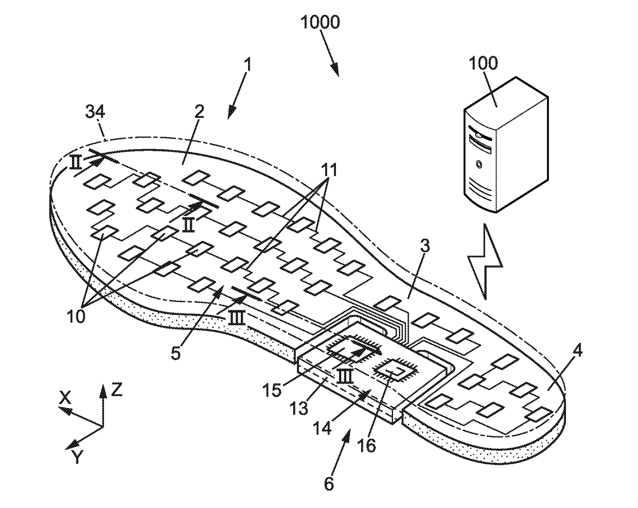
[0197]FIG. 5 illustrates the chip portion 6 of an insole 1 according to the invention.
[0198]On the example of FIG. 5, the chip support member 13 is provided with conductive tracks 18 on its upper face 13a and on its lower face 13b. In variant, conductive tracks 18 may be provided only on one of the upper face 13a and the lower face 13b.
[0199]The control and transmit electronics 14 are soldered on the chip support member 13, and in particular on the conductive tracks 18 provided on the chip support member 13.
[0200]In this first embodiment, the upper contacting tab 19 and the lower contacting tab 20 of the lower sheet are facing each other along the thickness direction Z.
[0201]The upper contacting tab 19 is in surface contact with the upper face 13a of the chip support member 13 and the lower contacting tab 20 is in surface contact with the lower face 13b of the chip support member 13.
[0202]In this embodiment, the whole thickness of the chip support member 13 is thus sandwiched betwe...
second embodiment
[0247]FIG. 8 illustrates the invention wherein the upper contacting tab 19 covers a majority of the upper face 13a of the chip support member 13 and the lower contacting tab 20 covers a majority of the lower face 13b of the chip support member 13.
[0248]In the example of FIG. 8, the upper contacting tab 19 entirely covers the upper face 13a of the chip support member 13 and the lower contacting tab 20 entirely covers the lower face 13b of the chip support member 13.
[0249]In this embodiment of the invention, the control and transmit electronics 14 are soldered on the upper contacting tab 19 and / or on the lower contacting tab 20.
[0250]In this second embodiment, the upper sheet 7 in particular comprises two conductive layers 7b, one on its upper face 7c and one on its lower face 7d.
[0251]The control and transmit electronic is soldered on the conductive layer 7b on the upper face 7c of the upper sheet 7. The conductive leads 19a connected to the upper electrodes 10a of the capacitive fo...
third embodiment
[0254]FIG. 9 illustrates the invention wherein only a portion of the thickness of the chip support member 13 is sandwiched between the upper and lower contacting tabs 19, 20.
[0255]To this aim, the chip support member 13 can be, for instance, a laminate comprising an upper section 23, a middle section 24 and a lower section 25.
[0256]The upper contacting tab 19 and the lower contacting tab 20 are laminated within the chip support member 13, between said upper section 23, middle section 24 and a lower section 25.
[0257]More precisely, the upper contacting tab 19 of the upper sheet 7 is sandwiched between the upper section 23 and the middle section 24 of the chip support member 13. The upper contacting tab 19 is thus in surface contact with the upper section 23 and with the middle section 24 of the chip support member 13. The upper face 7c of the upper contacting tab 19 is thus in surface contact with the upper section 23, and the lower face 7d of the upper contacting tab 19 is in surfac...
PUM
 Abstract
Description
Claims
Application Information
 - R&D Engineer
- R&D Manager
- IP Professional
- Industry Leading Data Capabilities
- Powerful AI technology
- Patent DNA Extraction
Browse by: Latest US Patents, China's latest patents, Technical Efficacy Thesaurus, Application Domain, Technology Topic, Popular Technical Reports.
© 2024 PatSnap. All rights reserved.Legal|Privacy policy|Modern Slavery Act Transparency Statement|Sitemap|About US| Contact US: help@patsnap.com


