Mask blank, phase shift mask and method for manufacturing semiconductor device

a technology of semiconductor devices and mask blanks, applied in the field of mask blanks, phase shift masks, and semiconductor device manufacturing methods, can solve the problems of reducing the thickness of the light shielding film, difficult to ensure the optical density required for the outer peripheral region of the transfer mask, and affecting the optical density of the transfer mask

Active Publication Date: 2018-09-06
HOYA CORP
View PDF0 Cites 2 Cited by
  • Summary
  • Abstract
  • Description
  • Claims
  • Application Information

AI Technical Summary

Benefits of technology

The present invention relates to a mask blank that can reduce the thickness of the light shielding film and solve the problem of ArF light fastness when using a transition metal silicide-based material for the light shielding film. The invention also addresses the issue of pattern change during long periods of use with the phase shift mask, even when exposed to ArF excimer laser exposure light. The technical effects of the invention are improved efficiency and accuracy in the manufacturing process of semiconductor devices.

Problems solved by technology

However, the phase shift film of the halftone-type phase shift mask has a function of transmitting the exposure light at a predetermined transmittance, and hence it is difficult to ensure the optical density required for the outer peripheral region of the transfer mask with the phase shift film alone.
However, as considered as a problem also in Patent Document 2, Patent Document 3, or the like, in recent years, it has been found that, when a MoSi-based (transition metal silicide-based) film is irradiated with ArF excimer laser exposure light (ArF exposure light) for a long period of time, a phenomenon in which the line width of a pattern of the MoSi-based film changes occurs.

Method used


Image

  • Mask blank, phase shift mask and method for manufacturing semiconductor device
  • Mask blank, phase shift mask and method for manufacturing semiconductor device
  • Mask blank, phase shift mask and method for manufacturing semiconductor device

Examples


first embodiment

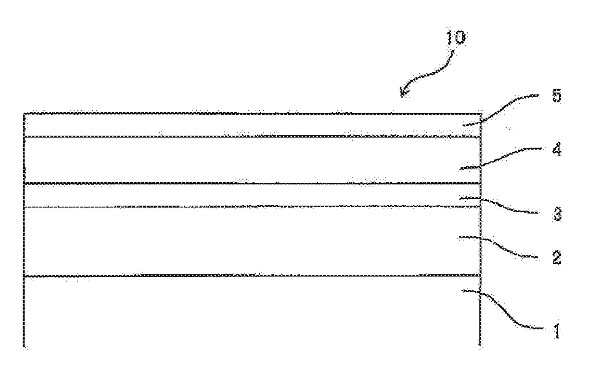
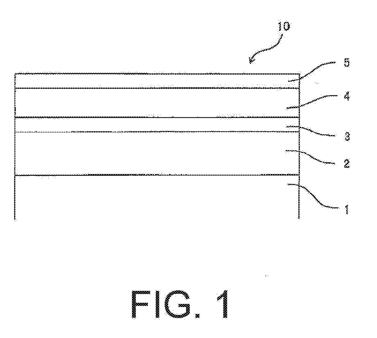
[0095]FIG. 1 is a sectional view for illustrating a layer configuration of a mask blank 10 according to a first embodiment of this invention. The mask blank 10 according to this invention illustrated in FIG. 1 has a structure in which a phase shift film 2, an etching stopper film 3, a light shielding film 4, and a hard mask film 5 are laminated on a transparent substrate 1 in the stated order.

[0096]Now, description of each layer is given.

[0097]>

[0098]The transparent substrate 1 is not particularly limited as long as the transparent substrate 1 has transparency to an ArF excimer laser. In this invention, a synthetic quartz substrate, or any of other various glass substrates (for example, soda lime glass or aluminosilicate glass) may be used. Of those various glass substrates, a synthetic quartz substrate has high transparency to ArF excimer laser or in a shorter wavelength region, and hence, is particularly suitable as a substrate for the mask blank of this invention to be used for f...

second embodiment

[0151]Next, a mask blank 10 according to a second embodiment of this invention is described. The mask blank 10 of the second embodiment has the same configurations as the mask blank 10 of the first embodiment except that the configuration of the phase shift film 2 differs from that of the mask blank 10 of the first embodiment. The same configurations as in the first embodiment are denoted by the same signs as in the first embodiment, and descriptions thereof are omitted or simplified herein. Accordingly, a description is given mainly of the phase shift film 2 of the mask blank 10 of the second embodiment below.

[0152]>

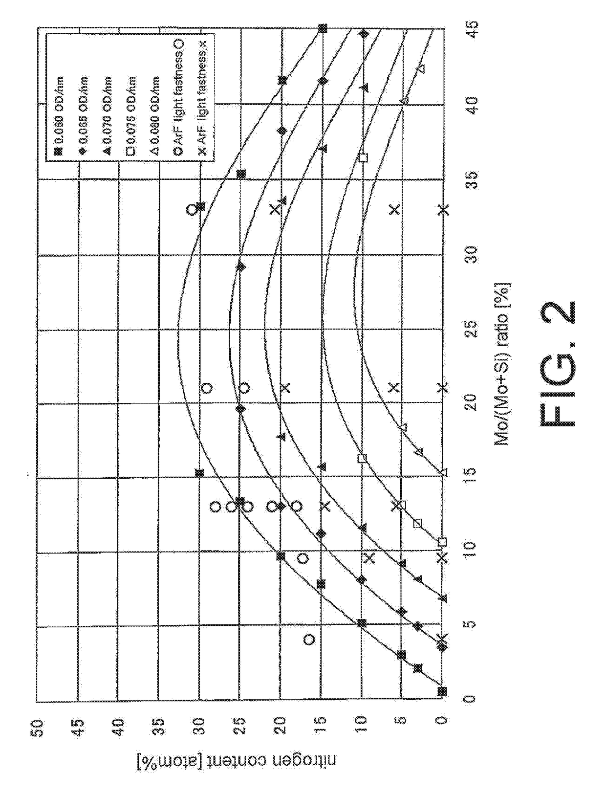
[0153]The phase shift film 2 of the second embodiment includes a surface layer and a layer other than the surface layer. The layer other than the surface layer of the phase shift film 2 is formed of a material which contains a transition metal, silicon, nitrogen, and oxygen, has a content of oxygen of 3 atom % or more, and satisfies a condition of the following expressi...

third embodiment

[0157]Next, a mask blank 10 according to a third embodiment of this invention is described. The mask blank 10 of the third embodiment has the same configurations as the mask blank 10 of the first embodiment except that the configuration of the phase shift film 2 differs from that of the mask blank 10 of the first embodiment. The same configurations as in the first embodiment are denoted by the same signs as in the first embodiment, and descriptions thereof are omitted or simplified herein. A description is given mainly of the phase shift film 2 of the mask blank of the third embodiment below.

[0158]>

[0159]The phase shift film 2 of the third embodiment includes a surface layer and a layer other than the surface layer. The layer other than the surface layer of the phase shift film 2 is formed of a material which contains a transition metal, silicon, nitrogen, and oxygen, has a content of oxygen of 3 atom % or more, and satisfies a condition of the following expression (C).

0.04×AS−0.06×...


PUM


Abstract

According to the present invention, provided is a mask blank (10), in which; a light shielding film (4) has a single layer structure or a laminate structure of a plurality of layers; at least one layer of the light shielding film (4) is formed of a material which contains a transition metal and silicon and is free from nitrogen and oxygen, or a material which contains a transition metal, silicon, and nitrogen and satisfies a condition of the following expression (1); a phase shift film (2) has a surface layer and a layer other than the surface layer; and the layer other than the surface layer is formed of a material which contains a transition metal, silicon, nitrogen, and oxygen, has a content of oxygen of 3 atom % or more, and satisfies a condition of the following expression (A).CN≤9.0×10⁻⁶×RM4−1.65×10⁻⁴×RM3−7.718×10⁻²×RM2+3.611×RM−21.084  Expression (1)0.04×AS−0.06×AM>1   Expression (A)

Description

TECHNICAL FIELD[0001]This invention relates to a mask blank, a phase shift mask, and a method of manufacturing a semiconductor device.BACKGROUND ART[0002]In general, in a manufacturing process for a semiconductor device, a fine pattern is formed using a photolithography method. In forming the fine pattern, a large number of substrates, which are called transfer masks, are generally used. Each of the transfer masks is generally obtained by forming a fine pattern formed of a metal thin film or the like on a transparent glass substrate. The photolithography method is used also for the production of the transfer mask.[0003]In forming a finer pattern of the semiconductor device, in addition to forming a finer mask pattern in a transfer mask, there is a need to use an exposure light source having a shorter wavelength in photolithography. In recent years, the wavelength of the exposure light source used in manufacturing the semiconductor device has become shorter from KrF excimer laser (wa...

Claims


Application Information

Patent Timeline
IPC IPC(8): G03F1/32G03F1/58G03F1/80G03F1/42G03F1/20H01L21/033
CPCG03F1/32G03F1/58G03F1/80G03F1/42G03F1/20H01L21/0337G03F7/70025G03F7/70283G03F1/38G03F1/48
Inventor MATSUMOTO, ATSUSHISHISHIDO, HIROAKIUCHIDA, TAKASHI
Owner HOYA CORP
Why Eureka
Try Eureka