Manufacturing method for flexible printed circuit board
a manufacturing method and printed circuit board technology, applied in the field of display, can solve the problems of excessive thickness of the fpc, increased signal transmission speed and frequency, and increased interference between signals, so as to reduce the thickness of the flexible insulating layer and the anti-emi layer and material consumption, reduce the thickness of the flexible printed circuit board with anti-emi structure, and reduce the production cost
- Summary
- Abstract
- Description
- Claims
- Application Information
AI Technical Summary
Benefits of technology
Problems solved by technology
Method used
Image
Examples
first embodiment
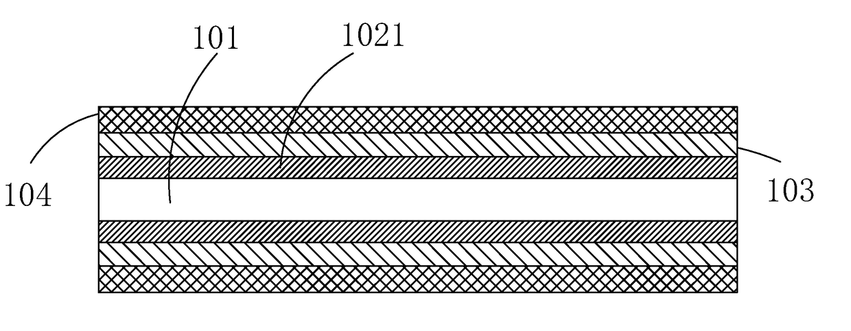
[0035]Specifically, refer to FIG. 3. In the present invention, the flexible printed circuit board is a double-sided single-layered flexible printed circuit board. In other words, a printed circuit is formed respectively on both sides of the flexible substrate 101, and each printed circuit comprises a conductive layer 1021. Correspondingly, in Step 2, a flexible insulating layer 103 is formed respectively on the conductive layer 1021 of each printed circuit; and in Step 3, an anti-EMI layer 104 is formed respectively on each flexible insulating layer 103. Preferably, the conductive layer 1021 is made of copper or gold, specifically, copper foil or gold foil so as to make the conductive layer 1021 flexible.
second embodiment
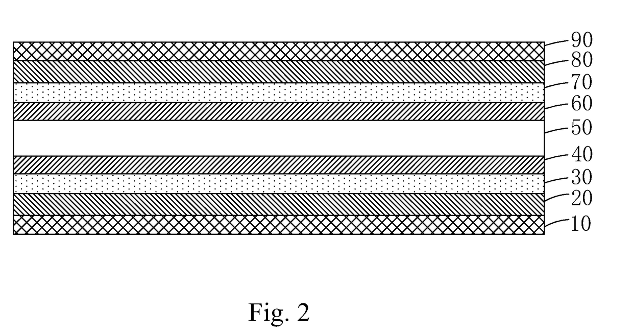
[0036]Specifically, refer to FIG. 4. In the present invention, the flexible printed circuit board is a double-sided multi-layered flexible printed circuit board. In other words, a printed circuit is formed respectively on both sides of the flexible substrate 101, and each printed circuit comprises a stack of conductive layers 1021, with an insulating protective layer 1022 disposed between two adjacent conductive layers 1021, an adhesive layer 1023 is disposed on a side of each insulating protective layer 1022 close to the flexible substrate 101. Correspondingly, in Step 2, a flexible insulating layer 103 is formed respectively on the conductive layer 1021 of each printed circuit farthest from the flexible substrate 101; and in Step 3, an anti-EMI layer 104 is formed respectively on each flexible insulating layer 103. Preferably, the conductive layer 1021 is made of copper or gold, specifically, copper foil or gold foil so as to make the conductive layer 1021 flexible. The insulating...
third embodiment
[0037]Specifically, refer to FIG. 5. In the present invention, the flexible printed circuit board is a single-sided single-layered flexible printed circuit board. In other words, a printed circuit is formed on a side of the flexible substrate 101, and the printed circuit comprises only a conductive layer 1021. Correspondingly, in Step 2, a flexible insulating layer 103 is formed on the conductive layer 1021 of the printed circuit; and in Step 3, an anti-EMI layer 104 is formed on the flexible insulating layer 103. Preferably, the conductive layer 1021 is made of copper or gold, specifically, copper foil or gold foil so as to make the conductive layer 1021 flexible.
PUM
| Property | Measurement | Unit |
|---|---|---|
| Length | aaaaa | aaaaa |
| Length | aaaaa | aaaaa |
| Thickness | aaaaa | aaaaa |
Abstract
Description
Claims
Application Information
 - R&D Engineer
- R&D Manager
- IP Professional
- Industry Leading Data Capabilities
- Powerful AI technology
- Patent DNA Extraction
Browse by: Latest US Patents, China's latest patents, Technical Efficacy Thesaurus, Application Domain, Technology Topic, Popular Technical Reports.
© 2024 PatSnap. All rights reserved.Legal|Privacy policy|Modern Slavery Act Transparency Statement|Sitemap|About US| Contact US: help@patsnap.com


