Radioactive contamination inspection apparatus
- Summary
- Abstract
- Description
- Claims
- Application Information
AI Technical Summary
Benefits of technology
Problems solved by technology
Method used
Image

Examples
first embodiment
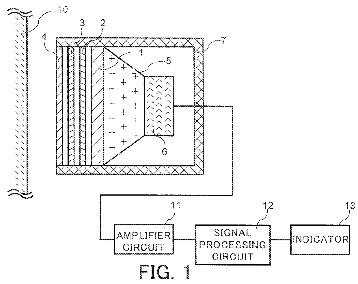
[0031]FIG. 1 is a diagram for illustrating a configuration of a radioactive contamination inspection apparatus according to a first embodiment of the present invention. The radioactive contamination inspection apparatus according to the first embodiment includes a plastic scintillator 1 configured to emit scintillation light through interaction with radioactive rays, a light guide 5 for guiding the scintillation light to a light receiving element 6, and a light shielding housing 7 for shielding the plastic scintillator 1, the light guide 5, and the light receiving element 6 from external light.
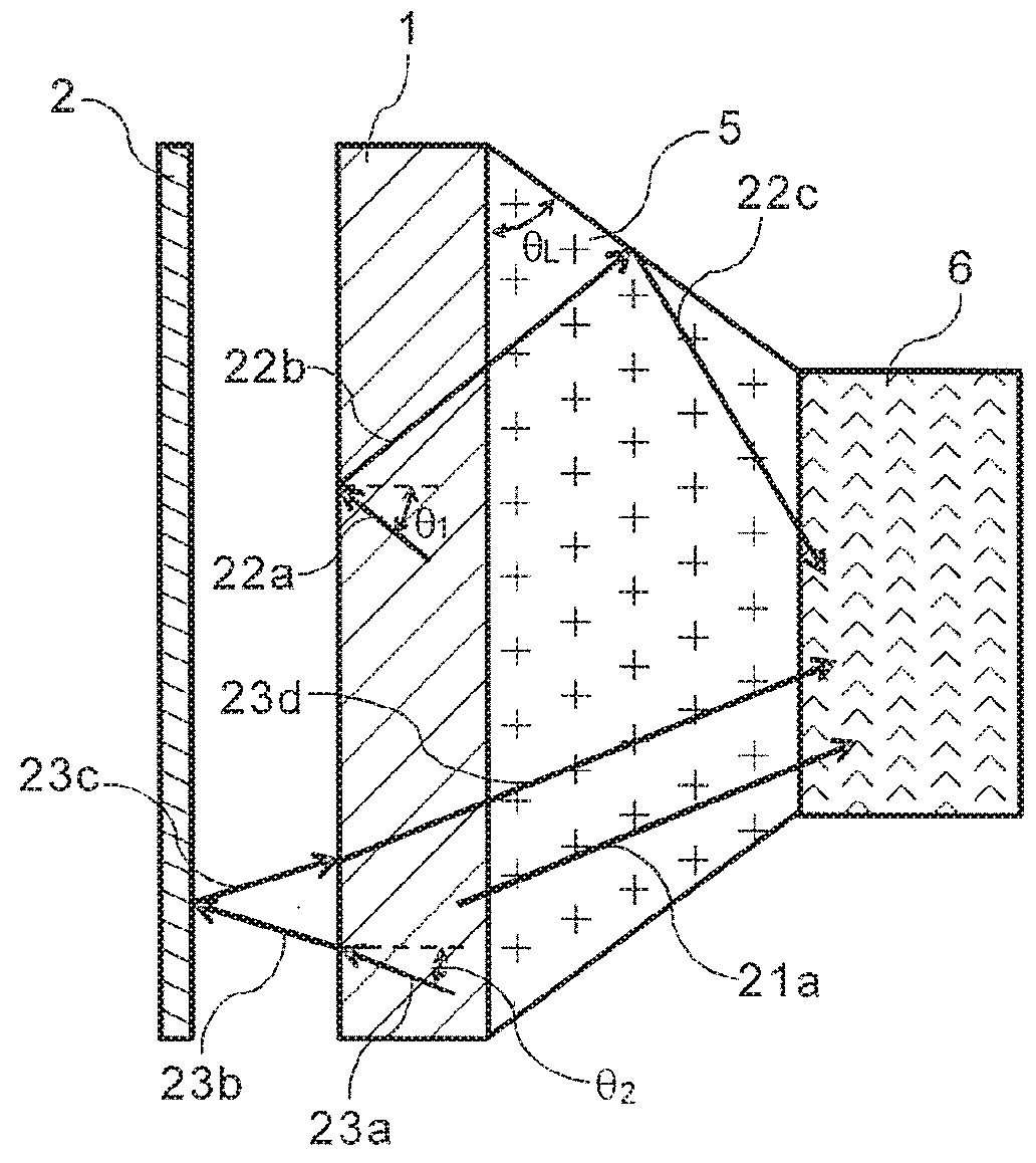
[0032]The light shielding housing 7 includes an incidence window on a measuring-object-side surface of the plastic scintillator 1. The incidence window has a thin film layer structure formed therein, which is configured by disposing a protective film 4, a light shielding film 3, and a reflective film 2 in the stated order from the outside. Further, the plastic scintillator 1 and the reflective...
second embodiment
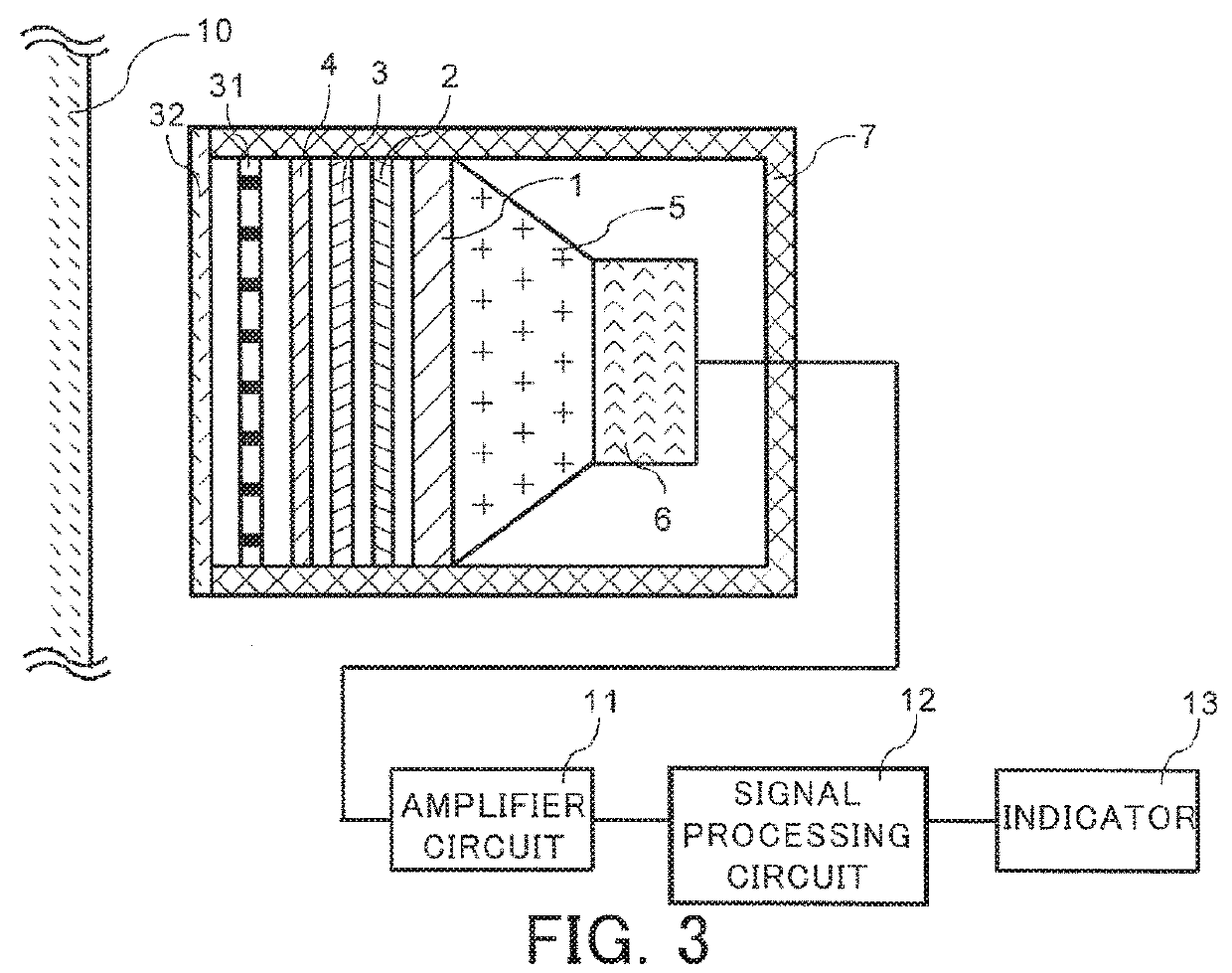
[0091]FIG. 3 is a diagram for illustrating a configuration of a radioactive contamination inspection apparatus according to a second embodiment of the present invention. The radioactive contamination inspection apparatus according to the second embodiment illustrated in FIG. 3 is different from the configuration of FIG. 1 in the first embodiment in terms of further including a protective screen 31 and an antistatic protective film 32 outside the protective film 4. Accordingly, the following description is given while focusing on those differences.
[0092]The protective screen 31 is mounted for the purpose of preventing damage on an incidence window when the radioactive contamination inspection apparatus is used in the outdoor or an object to be measured has many protrusions. The opening surface of the protective screen 31 has such a size as not to allow passage of a solid flying material and a protrusion that can damage the protective film 4, and has a structure having a large opening...
third embodiment
[0105]FIG. 7 is a diagram for illustrating a configuration of a radioactive contamination inspection apparatus according to a third embodiment of the present invention. The radioactive contamination inspection apparatus according to the third embodiment illustrated in FIG. 7 is different from that of FIG. 1 in the first embodiment in terms of further including a light emitting diode 41 between the reflective film 2 and the light shielding film 3. Accordingly, the following description is given while focusing on this difference.
[0106]The light emitting diode 41 is provided for the purpose of confirming the soundness of each of the light receiving element 6, the amplifier circuit 11, the signal processing circuit 12, and the indicator 13. As the light emitting diode 41, there can be used a light emitting diode configured to generate light having the same wavelength band as that of the scintillation light, or a light emitting diode configured to emit light having a different wavelength...
PUM
 Abstract
Description
Claims
Application Information
 - R&D
- Intellectual Property
- Life Sciences
- Materials
- Tech Scout
- Unparalleled Data Quality
- Higher Quality Content
- 60% Fewer Hallucinations
Browse by: Latest US Patents, China's latest patents, Technical Efficacy Thesaurus, Application Domain, Technology Topic, Popular Technical Reports.
© 2025 PatSnap. All rights reserved.Legal|Privacy policy|Modern Slavery Act Transparency Statement|Sitemap|About US| Contact US: help@patsnap.com