
Memory cells including vertical nanowire transistors

Active Publication Date: 2018-05-03
SYNOPSYS INC
View PDF6 Cites 43 Cited by
  • Summary
  • Abstract
  • Description
  • Claims
  • Application Information

AI Technical Summary

Benefits of technology

This patent describes the use of vertical nanowire columns in circuit structures. The vertical nanowire transistors have features that enable compact layouts, making them ideal for use in SRAM cells and logic cells. The circuit cells can be formed on conductive pads over an insulating layer, which can also serve as power conductors. The technical effects of this invention include improved performance, reduced latency, and improved reliability of circuit structures.

Problems solved by technology

The procedure of designing cells to be specified in a cell library is often a labor-intensive process, requiring highly skilled designers to manually design and refine the designs of the cells.
To fine tune finFET type circuits, complex reconfiguration of the fins or other structures may be required.
However, the area of the SRAM cell is relatively large in these examples.
For SRAM cells, the size of the cell is a critical factor in operating speed and in power consumption.
These issues relating to compact layouts also apply in many respects to logic cells, in general and other circuit components.

Method used


Image

  • Memory cells including vertical nanowire transistors
  • Memory cells including vertical nanowire transistors
  • Memory cells including vertical nanowire transistors

Examples


Embodiment Construction

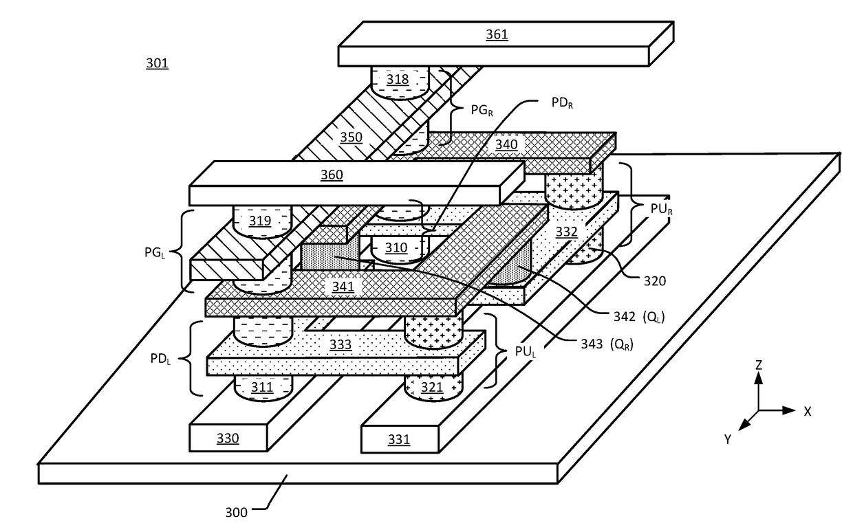
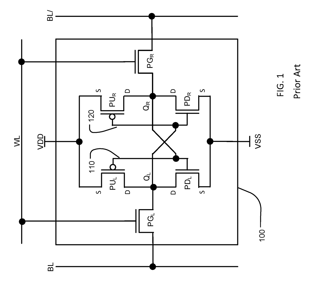
[0053]A detailed description of embodiments of the present invention is provided with reference to the figures. The following description will typically be with reference to specific structural embodiments and methods. It is to be understood that there is no intention to limit the invention to the specifically disclosed embodiments and methods but that the invention may be practiced using other features, elements, methods and embodiments. Preferred embodiments are described to illustrate the present invention, not to limit its scope, which is defined by the claims. Those of ordinary skill in the art will recognize a variety of equivalent variations on the description that follows. Like elements in various embodiments are commonly referred to with like reference numerals.

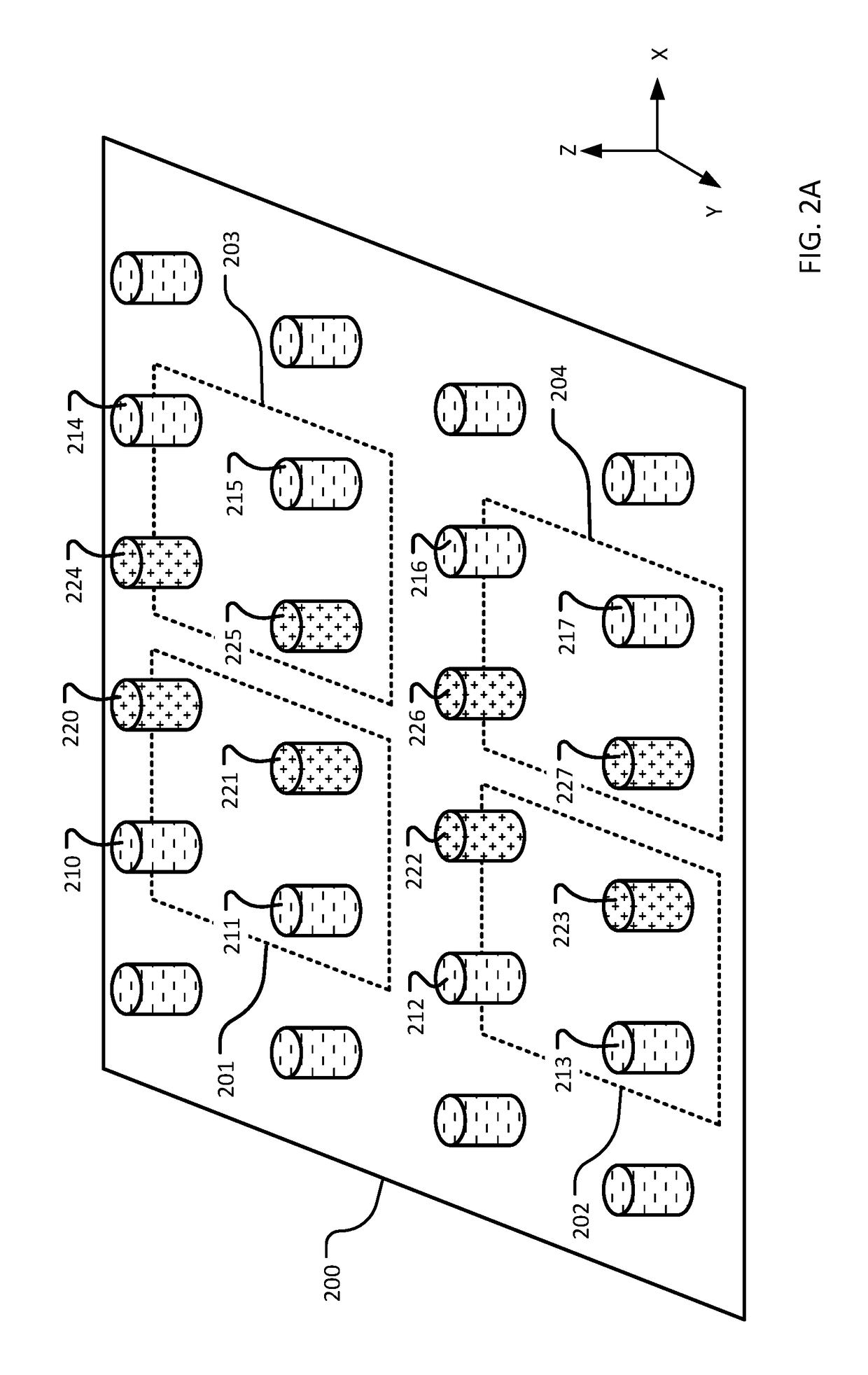
[0054]The term “nanowire” as used herein is a length of material, for example silicon, which has a minimum cross-sectional dimension of less than 10 nm, and which is sheathed by insulating material (which could be ai...


PUM


Abstract

A circuit including an SRAM cell with a set of vertical nanowire transistor columns is provided. Each member of the set includes a vertical nanowire transistor and at least one member of the set is a vertical nanowire transistor column including two vertical nanowire transistors in series. The set can consist of four vertical nanowire transistor columns, a first column including two n-type vertical nanowire transistors, a second column including two n-type vertical nanowire transistors, a third column including one p-type vertical nanowire transistor and a fourth column including one p-type vertical nanowire transistor. EDA tools for such circuits are also provided.

Description

PRIORITY APPLICATION[0001]This application claims the benefit of U.S. Provisional Patent Application No. 62 / 414,461 filed 28 Oct. 2016 which application is incorporated herein by reference.BACKGROUNDField of the Invention[0002]The present invention relates to memory cells, and more particularly relates to memory cells including nanowire transistors.Description of Related Art[0003]In the design of integrated circuits, standard cell libraries are often utilized. The process of designing the cells specified by entries in the cell libraries can be intensive, where trade-offs among variables such as the size of the cells, the drive power of the cells, the speed of the cells and so on, are made by adjusting the materials, geometry and size of the components of the cell. The procedure of designing cells to be specified in a cell library is often a labor-intensive process, requiring highly skilled designers to manually design and refine the designs of the cells.[0004]The development of finF...

Claims


Application Information

Patent Timeline
IPC IPC(8): H01L27/02H01L27/11H01L29/786H01L23/535G06F17/50
CPCH01L27/0207H01L27/1108H01L29/78642H01L29/78696H01L23/535G06F17/5072H01L27/0688H01L29/0676H01L21/823885H01L29/775H01L29/4238H01L29/66439H01L29/42392G06F30/392H10B10/12H10B10/125
Inventor MOROZ, VICTORKAWA, JAMILNGUYEN, THU
Owner SYNOPSYS INC
Learn More