Solid-state imaging device, method of driving solid-state imaging device, imaging system, and movable object
a technology of solid-state imaging and imaging device, which is applied in the direction of color television, television system, radio control device, etc., can solve the problem of image quality decline, and achieve the effect of suppressing the decline in image quality
- Summary
- Abstract
- Description
- Claims
- Application Information
AI Technical Summary
Benefits of technology
Problems solved by technology
Method used
Image
Examples
first embodiment
[0026]A solid-state imaging device and a method of driving the same according to a first embodiment of the present invention will be described with reference to FIG. 1 to FIG. 6.
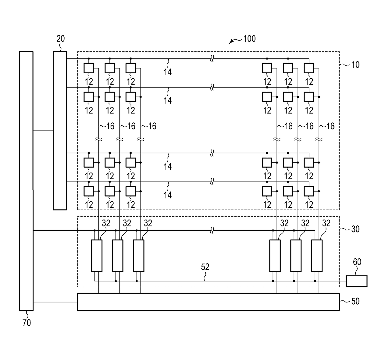
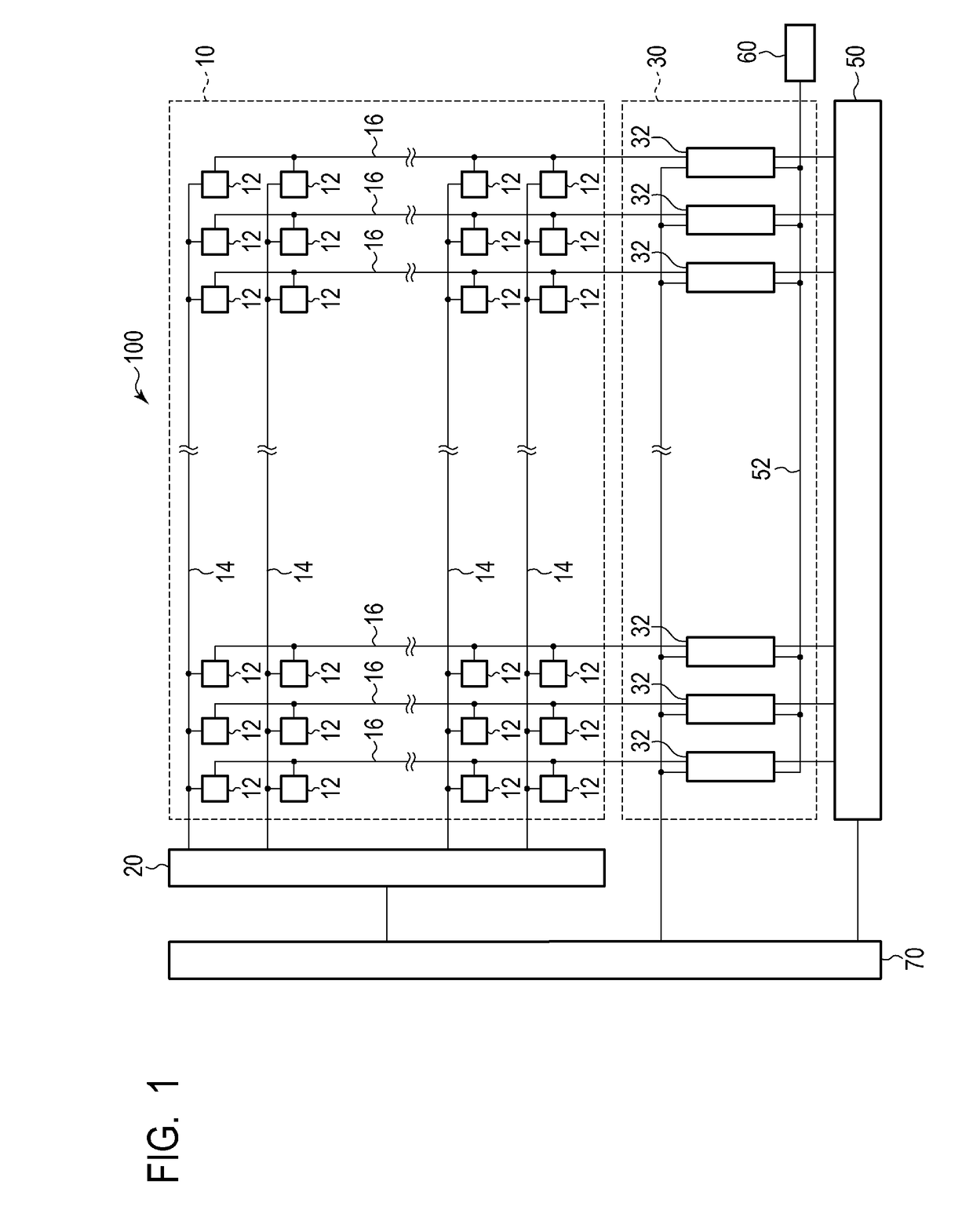
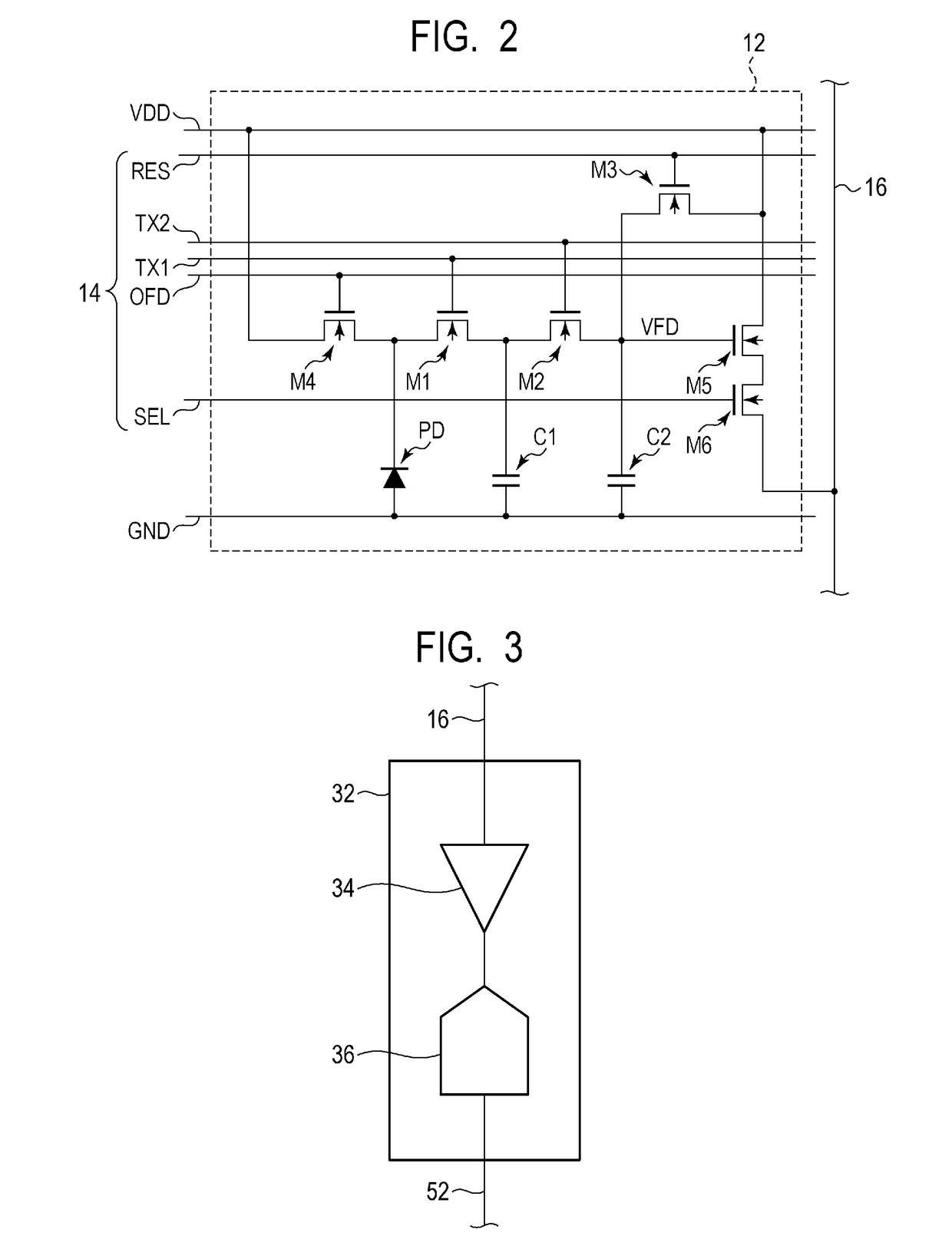
[0027]FIG. 1 is a block diagram illustrating a general configuration of a solid-state imaging device according to the present embodiment. FIG. 2 is a circuit diagram illustrating an example configuration of a pixel of the solid-state imaging device according to the present embodiment. FIG. 3 is a block diagram illustrating an example configuration of a column signal processing unit of the solid-state imaging device according to the present embodiment. FIG. 4 is a timing diagram illustrating a method of driving the solid-state imaging device according to the present embodiment. FIG. 5 and FIG. 6 are diagrams illustrating example settings of the number of transfers and the gain in the method of driving the solid-state imaging device according to the present embodiment.
[0028]First, the structure of the solid-st...
second embodiment
[0079]A solid-state imaging device and a method of driving the same according to a second embodiment of the present invention will be described with reference to FIG. 7 to FIG. 10. Components similar to those of the solid-state imaging device of the first embodiment are labeled with the same reference numerals, and the description thereof will be omitted or simplified.
[0080]FIG. 7 is a timing diagram illustrating an example drive operation of a solid-state imaging device when the number of transfers is two. FIG. 8 is a diagram illustrating an example setting of the number of transfers and a gain in the example drive operation of FIG. 7. FIG. 9 is a timing diagram illustrating the method of driving the solid-state imaging device according to the present embodiment. FIG. 10 is a diagram illustrating an example setting of the number of transfers and a gain in the method of driving the solid-state imaging device according to the present embodiment.
[0081]In the present embodiment, anothe...
third embodiment
[0093]A solid-state imaging device and a method of driving the same according to a third embodiment of the present invention will be described with reference to FIG. 11. Components similar to those of the solid-state imaging device of the first and second embodiments are labeled with the same reference numerals, and the description thereof will be omitted or simplified.
[0094]FIG. 11 is a timing diagram illustrating the method of driving the solid-state imaging device according to the present embodiment. In the present embodiment, another method of driving the solid-state imaging device according to the first embodiment illustrated in FIG. 1 to FIG. 3 will be described. In the present embodiment, a method of controlling accumulation time when distributing the accumulation time by using the transfer transistor M4 will be described.
[0095]As an example application to the first embodiment, it is assumed here that the ratio of the saturation charge amount QP of the photoelectric converter...
PUM
 Abstract
Description
Claims
Application Information
 - R&D
- Intellectual Property
- Life Sciences
- Materials
- Tech Scout
- Unparalleled Data Quality
- Higher Quality Content
- 60% Fewer Hallucinations
Browse by: Latest US Patents, China's latest patents, Technical Efficacy Thesaurus, Application Domain, Technology Topic, Popular Technical Reports.
© 2025 PatSnap. All rights reserved.Legal|Privacy policy|Modern Slavery Act Transparency Statement|Sitemap|About US| Contact US: help@patsnap.com


