Conductive film, touch panel sensor, and touch panel
a technology of touch panel sensor and conductive film, which is applied in the field of conductive film, touch panel sensor, touch panel, etc., can solve the problems of reducing the conductive characteristics of metal thin wires to be formed, and achieve the effect of enhancing the invention effect, excellent maintaining the transparency of conductive film, and visually recognizing the display without discomfor
- Summary
- Abstract
- Description
- Claims
- Application Information
AI Technical Summary
Benefits of technology
Problems solved by technology
Method used
Image
Examples
examples
[0235]Hereinafter, the invention will be described in more detail using examples. However, the invention is not limited thereto.
[0236](Preparation of To-Be-Plated Layer Forming Composition 1 (Hereinafter, also Referred to as Composition 1))
[0237]A polyacrylic acid (manufactured by Wako Pure Chemical Industries, Ltd., weight average molecular weight: 8,000 to 12,000), a tetrafunctional acrylamide, a polymerization initiator, a fluorine-based surfactant (trade name “Irgacure 127”, manufactured by BASF SE), and isopropanol were used to prepare a liquid in accordance with the composition of Table 1, and thus a composition 1 was obtained.
[0238]The tetrafunctional acrylamide is a compound represented by Formula (A). In Formula (A), R represents a hydrogen atom.
[0239]In Table 1, the content of each component is displayed in mass % with respect to a total amount of the composition.
TABLE 1Table 1Composition 1Polyacrylic Acid1.35Tetrafunctional Acrylamide0.9Polymerization Initiator0.045Fluori...
example a 1
[0240]On a substrate (trade name “LUMIRROR U48”, polyethylene terephthalate film, long film, manufactured by TORAY INDUSTRIES, INC.), the composition 1 was applied by roll coating to form a film having a thickness of 600 nm, and the film was dried by an oven at 80° C. to form a layer for forming a to-be-plated layer on the substrate. The substrate having the layer for forming a to-be-plated layer formed thereon (substrate with layer for forming to-be-plated layer) was wound into a roll. No blocking was observed in a case where the substrate with a layer for forming a to-be-plated layer was wound.
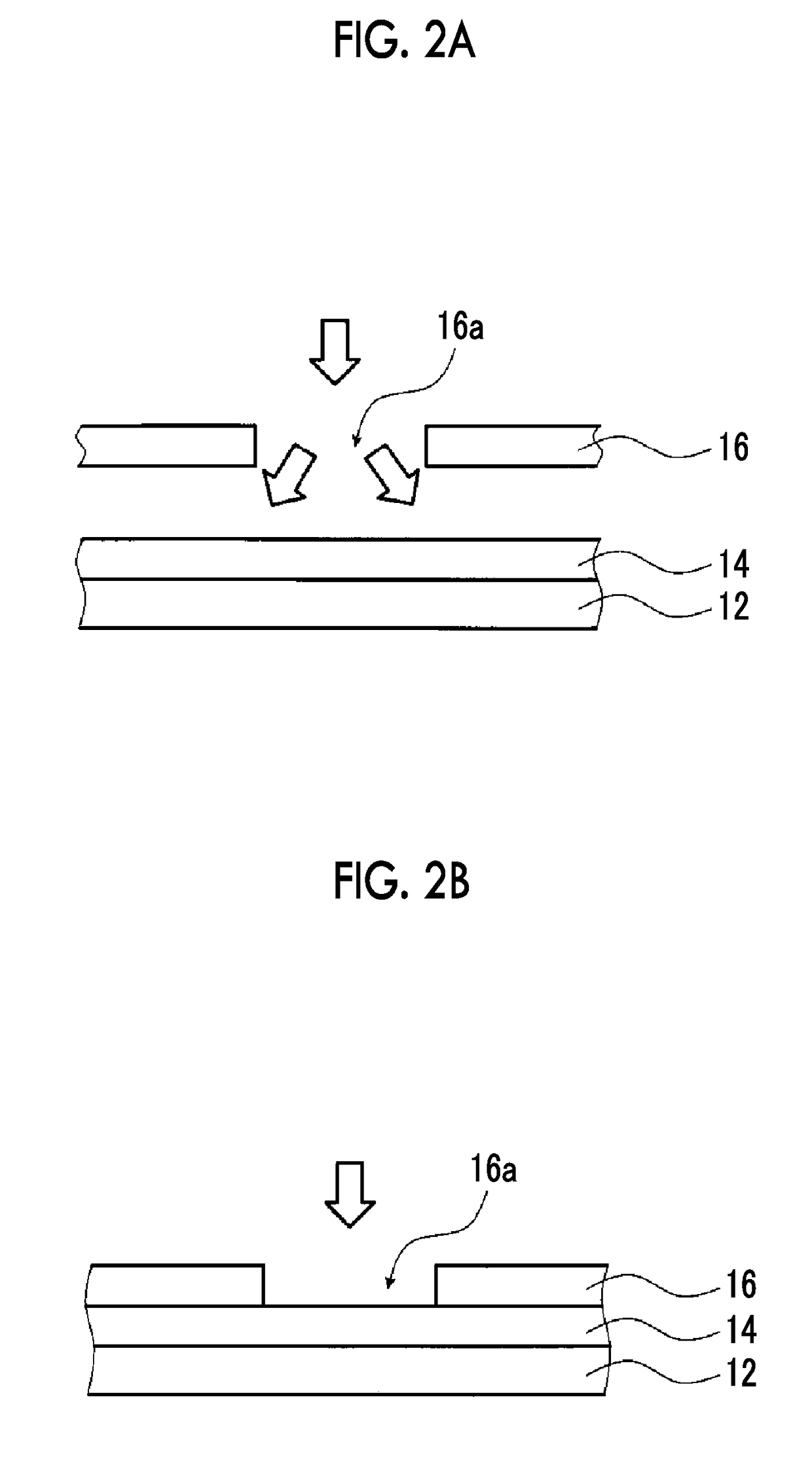
[0241]Then, the roll was unwound to place the substrate with a layer for forming a to-be-plated layer in a vacuum chamber, and a photomask (hard mask) having openings with a thin-line mesh pattern having a line width of 3 μm and the layer for forming a to-be-plated layer were brought into close contact with each other in vacuum. Next, the layer for forming a to-be-plated layer was irradiated...
example a2
[0246]A conductive film was manufactured according to the same procedure as Example A1, except that a to-be-plated layer forming composition 2 prepared according to the following procedure was used in place of the composition 1.
PUM
| Property | Measurement | Unit |
|---|---|---|
| Length | aaaaa | aaaaa |
| Length | aaaaa | aaaaa |
| Width | aaaaa | aaaaa |
Abstract
Description
Claims
Application Information
 - R&D
- Intellectual Property
- Life Sciences
- Materials
- Tech Scout
- Unparalleled Data Quality
- Higher Quality Content
- 60% Fewer Hallucinations
Browse by: Latest US Patents, China's latest patents, Technical Efficacy Thesaurus, Application Domain, Technology Topic, Popular Technical Reports.
© 2025 PatSnap. All rights reserved.Legal|Privacy policy|Modern Slavery Act Transparency Statement|Sitemap|About US| Contact US: help@patsnap.com


