
High power semiconductor device

a semiconductor and high-power technology, applied in the direction of semiconductor devices, basic electric elements, electrical appliances, etc., can solve the problems of significant leakage current, defect, and more strain in the aluminum gallium nitride layer of the transistor, and achieve the effect of reducing the turn-on voltage and turn-on resistance, increasing the breakdown voltage, and high power

Active Publication Date: 2018-02-01
EPISTAR CORP
View PDF4 Cites 8 Cited by
  • Summary
  • Abstract
  • Description
  • Claims
  • Application Information

AI Technical Summary

Benefits of technology

The patent text describes a new semiconductor device that has two diodes connected in parallel and a schottky contact on a channel layer. This design reduces the voltage and resistance when the device is turned on, which makes it more durable.

Problems solved by technology

While operating a high electron mobility transistor, a high electric field concentrates at edges of schottky metal contacts of a gate, which results in more strain in an aluminum gallium nitride layer of the transistor.
Further, when the transistor operates under a drain-to-gate threshold voltage, defects occur due to the reasons above.
Additionally, these defects become deep-level traps that generate electrons tunnels which cause significant leakage currents.
Therefore, a breakdown of the transistor occurs earlier than expected and the breakdown voltage of the transistor cannot be increased.

Method used


Image

  • High power semiconductor device
  • High power semiconductor device
  • High power semiconductor device

Examples


first embodiment

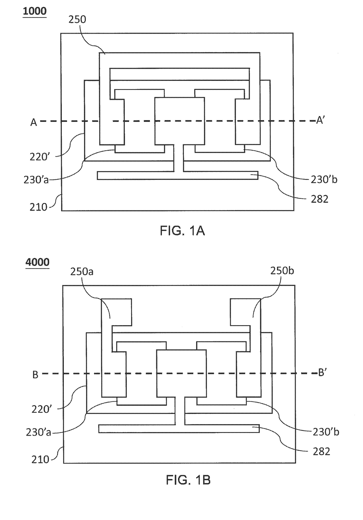
[0019]FIG. 1A shows a top view of a high power semiconductor device 1000 in accordance with the present application. FIG. 2F shows a top view taken along a line A-A′ of the high power semiconductor device 1000 as shown in FIG. 1A.

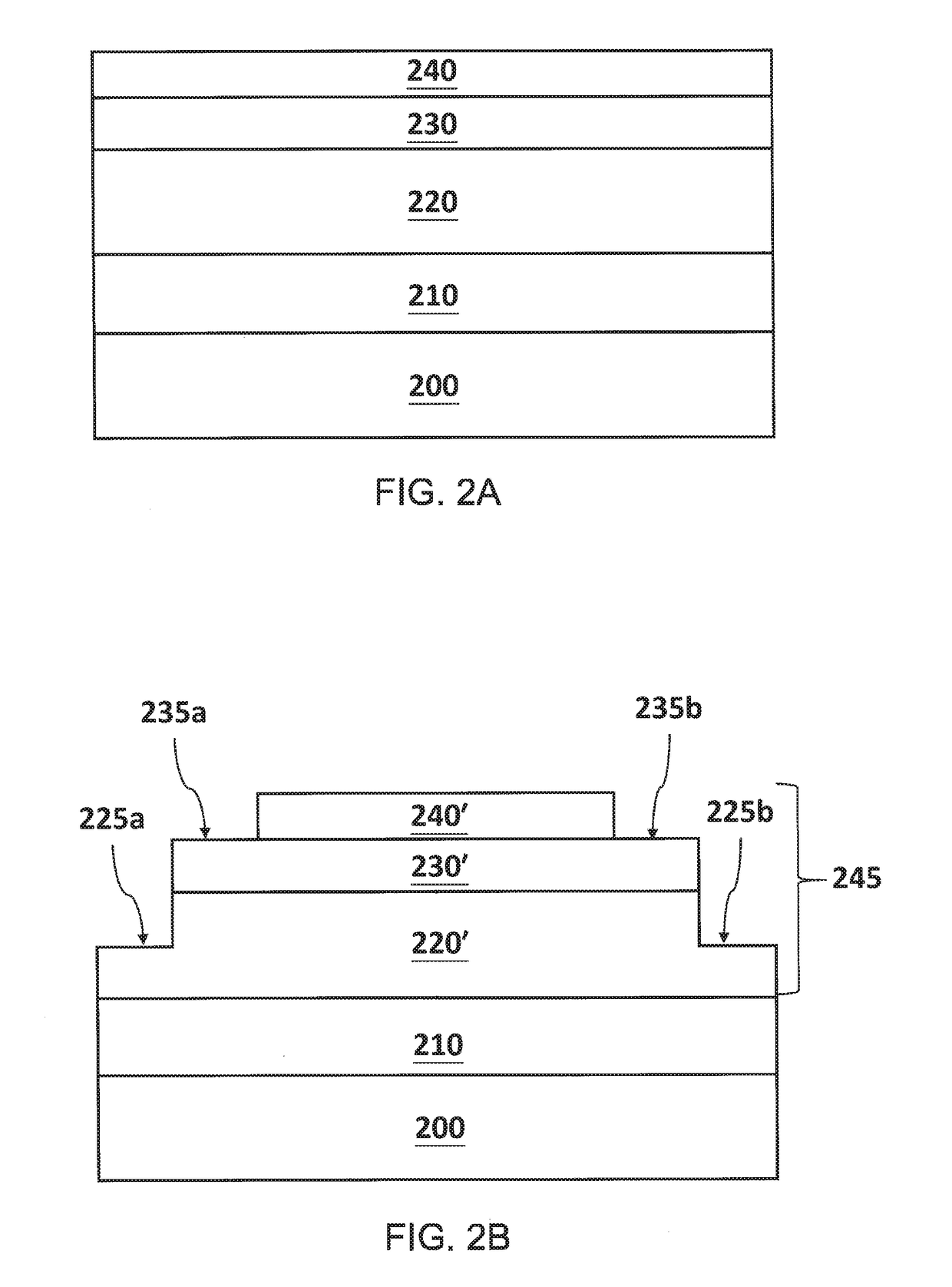
[0020]A description accompanied with FIG. 2A to FIG. 2F is provided in the following to explain a manufacturing process of the high power semiconductor device 1000 in accordance with the first embodiment of the present application.

[0021]In FIG. 2A, a substrate 2000 is provided, and a buffer layer 210, a channel layer 220, a barrier layer 230, and a cap layer 240 which can be a semiconductor layer with a conductivity type are deposited in sequence on the substrate 2000 by an epitaxial process. Herein, the substrate 200 can be a conductive substrate or an insulating substrate and a material of the substrate 200 can include sapphire, silicon carbide, or silicon. A material of the buffer layer 210 can include a IIIA-VA material, for example, aluminum nitride, g...

fourth embodiment

[0034]FIG. 1B shows a top view of a high power semiconductor device 4000 in accordance with the present application. FIG. 5 shows a cross-sectional view taken along a line B-B′ of the high power semiconductor device 4000 as shown in FIG. 1B.

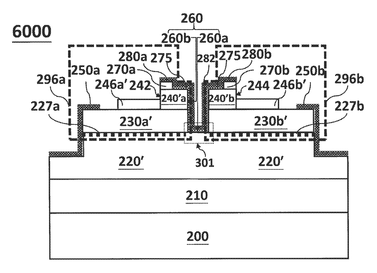
[0035]FIG. 5 shows a cross-sectional view of the high power semiconductor device 4000 in accordance with the fourth embodiment of the present application. The high power semiconductor device 4000 shown in FIG. 5 is similar to the high power semiconductor device 1000 disclosed in the first embodiment and includes a structure disposed on a substrate 200 and a buffer layer 210 and constructed by a channel layer 220′, a first barrier layer 230′a, a second barrier layer 230′b, a first cap layer 240′a, a second cap layer 240′b, a first ohmic contact layer 270a, a second ohmic contact layer 270b, a first cathode 250a, a second cathode 250b, a first anode 280a, and a second anode 280b. Herein, the difference between the high power semiconductor device 40...


PUM


Abstract

This application provides a high power semiconductor device, which is characterized by forming two diodes connected in parallel and a schottky contact on a channel layer to lower the turn-on voltage and turn-on resistance of the high power semiconductor device at the same time and to enhance the breakdown voltage.

Description

REFERENCE TO RELATED APPLICATION[0001]The present application claims the right of priority based on TW application Serial No. 105124363, filed on Aug. 1, 2016, and the content of which is hereby incorporated by reference in its entirety.FIELD OF THE INVENTION[0002]The present application is related to a high power semiconductor device, and more particularly, to a high power semiconductor device with high electron mobility.DESCRIPTION OF THE PRIOR ART[0003]A high electron mobility transistor is a heterostructure including two materials with different energy band gap, for example, a heterostructure consisting of an aluminum gallium nitride layer and a gallium nitride layer that can cause a spontaneous polarization and a piezoelectric polarization. Under a condition that the heterostructure is undoped, a two dimensional electron gas with high concentration is formed at an interface between the aluminum gallium nitride layer and the gallium nitride layer, so that a speed of carriers is ...

Claims


Application Information

Patent Timeline
Patent Type & Authority Applications(United States)
IPC IPC(8): H01L29/778H01L29/20H01L29/06H01L29/08H01L29/423H01L29/66H01L29/10H01L29/205
CPCH01L29/7787H01L29/1054H01L29/2003H01L29/205H01L29/0891H01L21/0254H01L29/0847H01L29/66462H01L29/0611H01L29/868H01L21/02458H01L29/4236H01L29/0619H01L29/7786H01L29/41766H01L29/42316H01L29/1066
Inventor CHEN, MING-CHINLIN, YI-CHIHTU, SHANG-JU
Owner EPISTAR CORP
Learn More