Monolayer film mediated precision film deposition

a technology of monolayer film and precision film, applied in the field of precision deposition technique for forming thin films, can solve the problems of greater challenges in scaling efforts

Active Publication Date: 2018-01-25
TOKYO ELECTRON LTD
View PDF3 Cites 1 Cited by
  • Summary
  • Abstract
  • Description
  • Claims
  • Application Information

AI Technical Summary

Benefits of technology

[0007]Note that this summary section does not specify every embodiment and / or incrementally novel aspect of the present disclosure or claimed invention. Instead, this summary only provides a preliminary discussion of different embodiments and corresponding points of novelty over conventional techniques. For additional details and / or possible perspectives of the invention and embodiments, the reader is directed to the Detailed Description section and corresponding figures of the present disclosure as further discussed below.

Problems solved by technology

Scaling efforts have greatly increased the number of transistors per unit area in 2D circuits, yet scaling efforts are running into greater challenges as scaling enters single digit nanometer semiconductor device fabrication nodes.

Method used


Image

  • Monolayer film mediated precision film deposition
  • Monolayer film mediated precision film deposition
  • Monolayer film mediated precision film deposition

Examples


Embodiment Construction

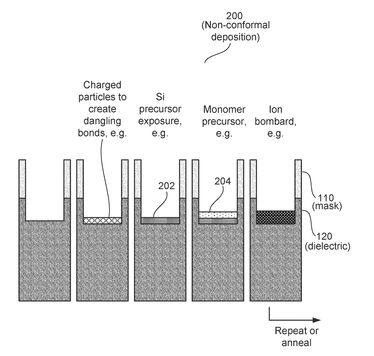
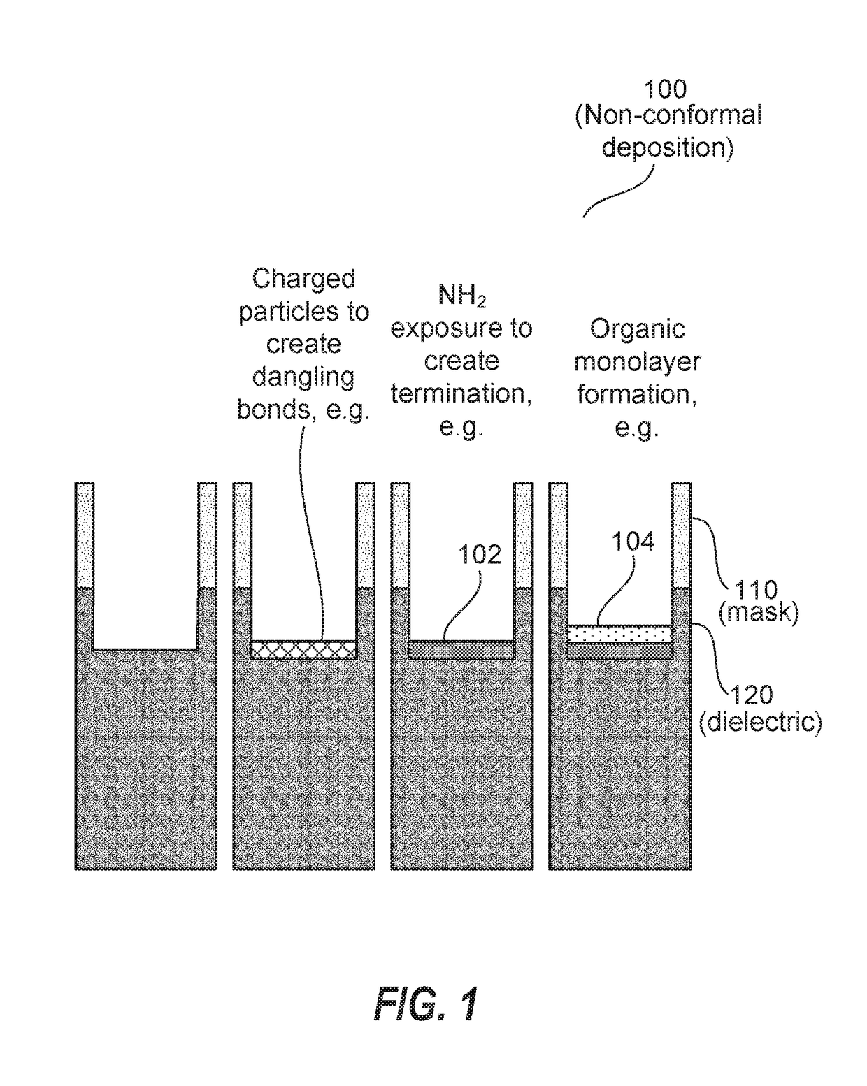
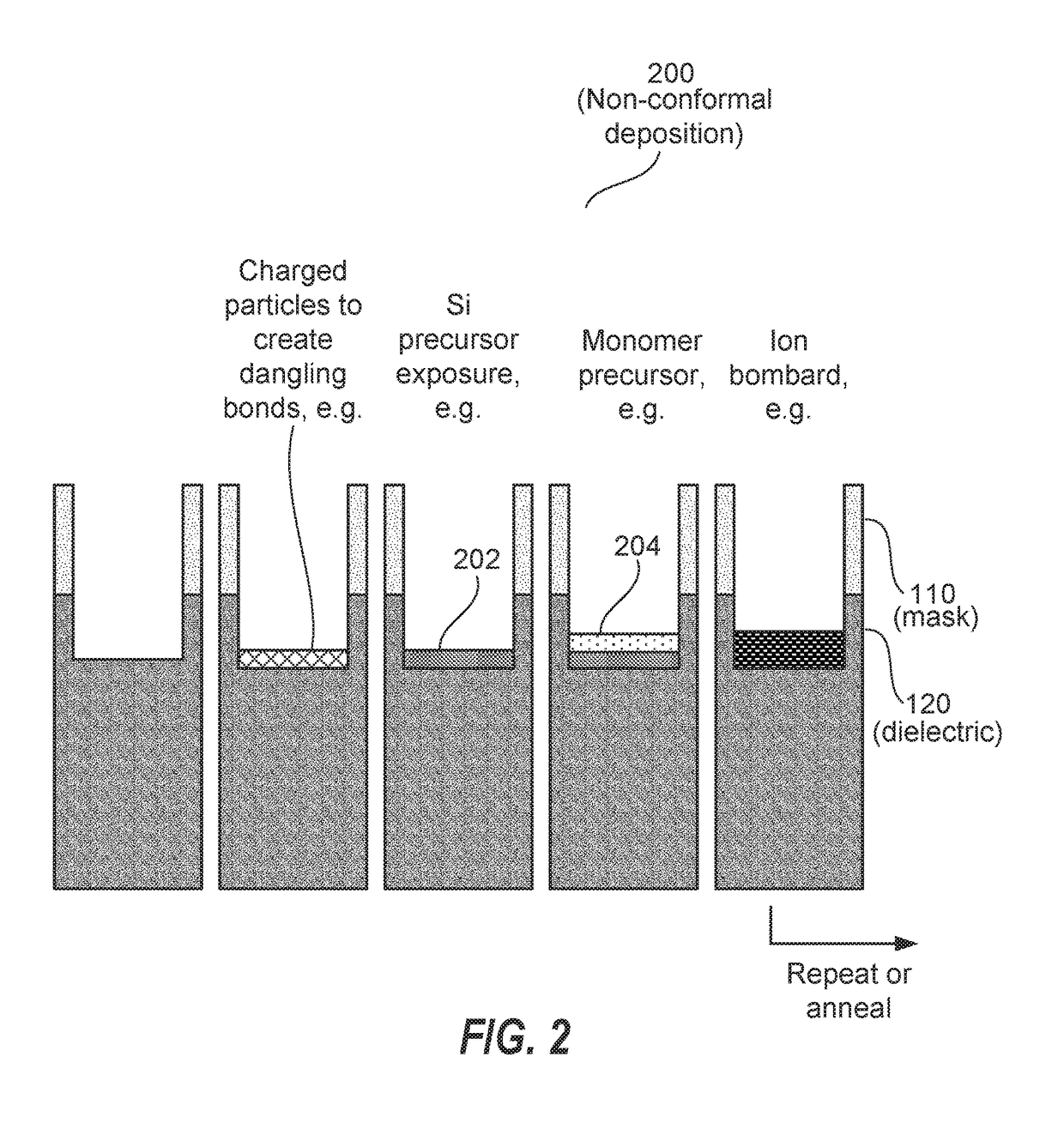
[0012]Techniques herein pertain to device fabrication using precision deposition techniques. One such material requiring precision deposition for current and future device technology is SiC. SiC films have many applications in semiconductor device manufacturing ranging from power electronics to barrier film applications. To that extent there is a host of CVD (chemical vapor deposition) and emerging ALD (atomic layer deposition) techniques for their deposition. CVD methods, generally at high temperature, typically employ precursors, such as dichlorosilane (DCS) as a silicon precursor and a hydrocarbon (CH4, C2H2, etc.) as a carbon precursor.

[0013]ALD, on the other hand, is challenging, wherein a surface pre-treatment or self-limiting surface reaction with the silicon surface is necessary to deposit an organic material. Organic structures are not typically deposited in a self-limiting manner over silicon without the introduction of an exotic functional group.

[0014]One example includes...


PUM

PropertyMeasurementUnit
adsorptionaaaaaaaaaa
temperatureaaaaaaaaaa
temperaturesaaaaaaaaaa

Abstract

A method of forming a thin film is described. The method includes treating at least a portion of a surface exposed on a substrate with an adsorption-promoting agent to alter a functionality of the exposed surface and cause subsequent adsorption of an organic precursor, and thereafter, adsorbing the organic precursor to the functionalized surface to form a carbon-containing film. Then, at least a portion of the surface of the carbon-containing film is exposed to an ion flux to mix the adsorbed carbon-containing film with the material of the underlying substrate and form a mixed film.

Description

CROSS-REFERENCE TO RELATED APPLICATIONS[0001]This application is related to and claims priority to U.S. Provisional Patent Application Ser. No. 62 / 366,516 filed on Jul. 25, 2016, the entire contents of which are herein incorporated by reference.FIELD OF INVENTION[0002]The invention relates to a method for forming a thin film, and more particularly, a precision deposition technique for forming a thin film for electronic device applications.BACKGROUND OF THE INVENTION[0003]The present invention relates to a method of manufacturing a semiconductor device such as an integrated circuit and transistors and transistor components for an integrated circuit. In the manufacture of a semiconductor device (especially on the microscopic scale), various fabrication processes are executed such as film-forming depositions, etch mask creation, patterning, material etching and removal, and doping treatments, are performed repeatedly to form desired semiconductor device elements on a substrate. Histori...

Claims


Application Information

Patent Timeline
Patent Type & Authority Applications(United States)
IPC IPC(8): H01L21/02C23C14/02C23C16/32H01L21/3105C23C16/455
CPCH01L21/02299H01L21/02167H01L21/0228H01L21/02318C23C16/45542C23C16/45553C23C16/325C23C14/024H01L21/31051H01L21/02274H01L21/02315H01L21/02205H01L21/02381H01L21/324
Inventor VENTZEK, PETERRANJAN, ALOK
Owner TOKYO ELECTRON LTD
Why Eureka
Try Eureka