Method for producing a passivated semiconductor structure based on group iii nitrides, and one such structure

a semiconductor structure and passivating technology, applied in the direction of basic electric elements, semiconductor devices, electrical equipment, etc., can solve the problems of deteriorating luminescence output, dislocation of threading, and lack of means to achieve i

Active Publication Date: 2018-01-11
CENT NAT DE LA RECHERCHE SCI
View PDF6 Cites 3 Cited by
  • Summary
  • Abstract
  • Description
  • Claims
  • Application Information

AI Technical Summary

Benefits of technology

[0027]The fact of depositing a crystalline layer that covers the entire surface of a layer based on group III nitrides of the semiconductor structure makes it possible to passivate totally the surface of this layer based on group III nitrides and thus to prevent any oxidation reaction of the latter. This enables the storage of the semiconductor structure covered with the crystalline passivation layer prior to the deposition of additional layers of the semiconductor structure based on group III nitrides.
[0029]The step of deposition of a crystalline passivation layer based on silicon moreover enables a later growth of a crystalline layer thereon, for example a layer based on group III nitride, whereas an amorphous nanoporous layer covering the layer based on group III nitride would not enable this later growth. The described diffraction image corresponds to a hexagonal periodical arrangement turned by 30° with respect to the lattice of the layer based on group III nitride and of lattice parameter √{square root over (3)} times greater than the lattice parameter of the lattice of the layer based on group III nitride, which makes it possible to favour this later growth of a crystalline layer.

Problems solved by technology

These threading dislocations are particularly disadvantageous in the case of semiconductor structures forming light emitting devices based on semiconductor materials of group III nitrides since threading dislocations increase leakage currents and deteriorate the luminescence output of these light emitting devices.
A drawback of the mentioned growth technique with the nano-mask of SiNx relates to the fact that oxidation reactions may take place at the surface of the buffer layer not covered by the SiNx layer.
Another drawback of this technique relates to the fact that no means exist for making it possible to define the optimal duration of the step of deposition of the nanoporous SiNx layer.
The size of the openings and the density thereof are non-measurable quantities, thus the determination of the optimal duration of the step of deposition of the nanoporous SiNx layer may thus only be obtained in an empirical manner by carrying out successive tests, which have to be reiterated each time that one of the growth parameters (i.e. substrate, reactor, etc.) is modified, which is time consuming and especially does not make it possible to carry out a generic method, that is to say applicable in a general manner.

Method used


Image

  • Method for producing a passivated semiconductor structure based on group iii nitrides, and one such structure
  • Method for producing a passivated semiconductor structure based on group iii nitrides, and one such structure
  • Method for producing a passivated semiconductor structure based on group iii nitrides, and one such structure

Examples


example of

Production Method

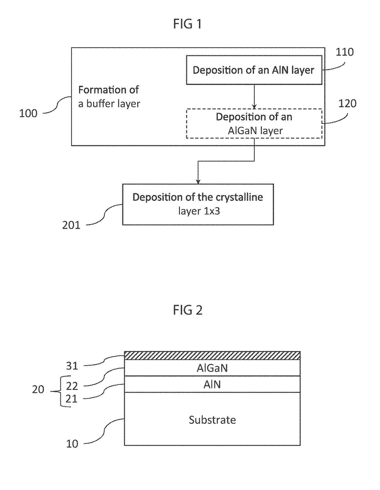
[0148]An example of method according to the invention will now be described.

[0149]The silicon substrate used has a crystallographic orientation (111).

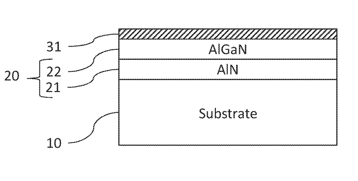
[0150]A buffer aluminium nitride AlN layer is formed by molecular beam epitaxy on the silicon substrate. The formation of the buffer layer is interrupted when the thickness thereof is comprised between 10 and 200 nm.

[0151]The step of deposition of the crystalline layer 1×3 is then carried out. A surface treatment of the buffer layer by molecular beam epitaxy is implemented using silicon atoms and molecules of ammonia NH3. This surface treatment leads to the formation of a new well-defined epi-ready crystalline structure, measurable and identifiable by electron diffraction.

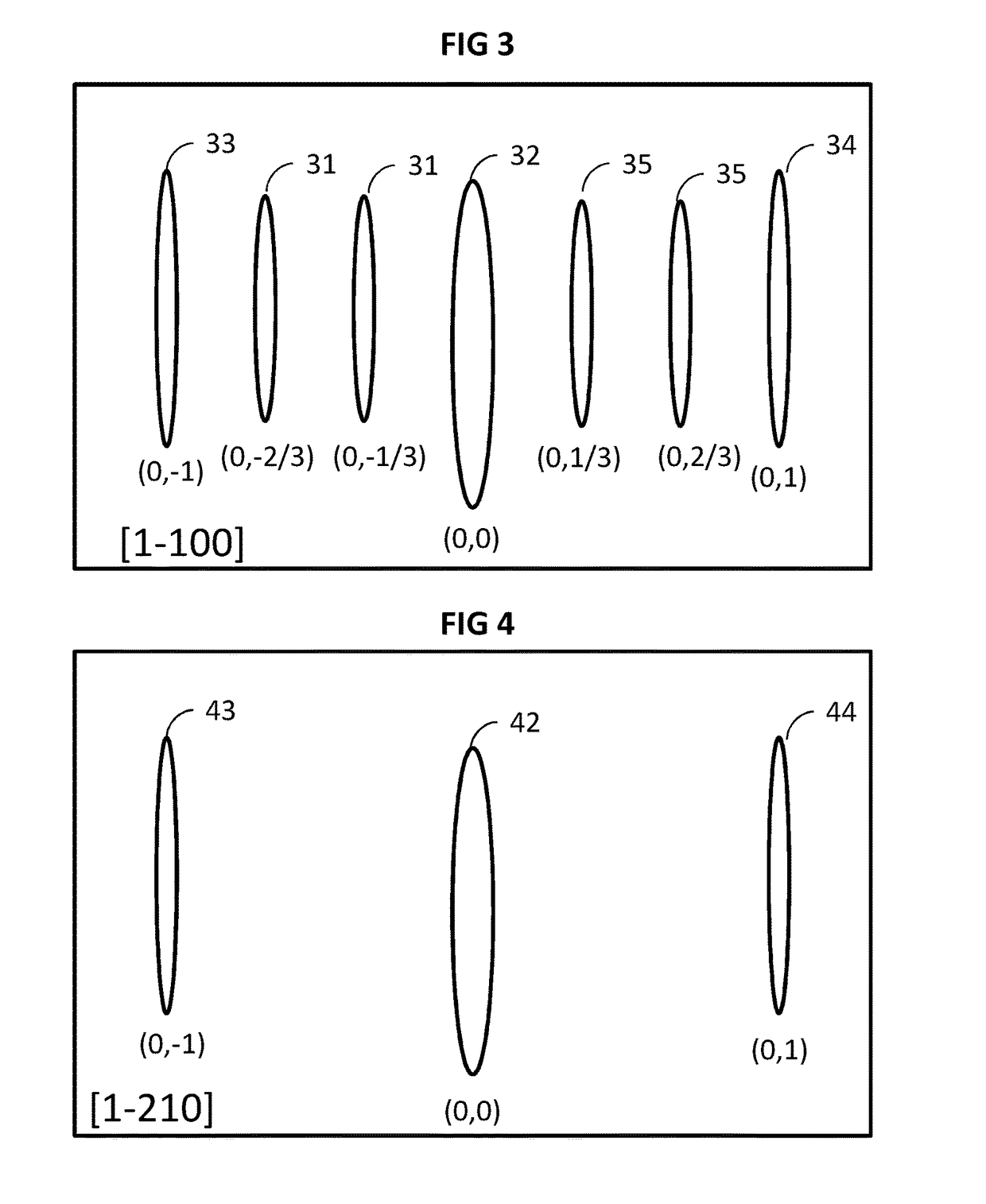
[0152]During the deposition of the crystalline layer, the surface is observed by an electron diffraction technique consisting of sending at grazing incidence a beam of monokinetic electrons onto the crystalline layer in the course of formation in orde...


PUM


Abstract

The invention relates to a method for producing a semiconductor structure, characterised in that the method comprises a step (201) of depositing a crystalline passivation layer continuously covering the entire surface of a layer based on group III nitrides, said crystalline passivation layer, which is deposited from a precursor containing silicon atoms and a flow of nitrogen atoms, consisting of silicon atoms bound to the surface of the layer based on group III nitrides and arranged in a periodical arrangement such that a diffraction image of said crystalline passivation layer obtained by grazing-incidence diffraction of electrons in the direction [1-100] comprises:two fractional order diffraction lines (0, −⅓) and (0, −⅔) between the central line (0, 0) and the integer order line (0, −1), andtwo fractional order diffraction lines (0, ⅓) and (0, ⅔) between the central line (0, 0) and the integer order line (0, 1).

Description

FIELD OF THE INVENTION[0001]The invention relates to a method for producing a semiconductor structure based on group III nitrides, and one such semiconductor structure.PRESENTATION OF THE PRIOR ART[0002]Semiconductor materials based on group III nitrides of the periodic table—such as materials based on gallium nitride GaN—occupy an increasingly important place in the electronics and optoelectronics fields, notably for the production of light emitting diodes.[0003]Existing methods for producing a semiconductor structure based on group III nitrides, such as gallium nitride GaN, on a substrate, for example made of silicon or sapphire, generally result in an important threading dislocation density linked to the difference in lattice parameter between the host substrate and semiconductor materials based on group III nitrides. These threading dislocations are particularly disadvantageous in the case of semiconductor structures forming light emitting devices based on semiconductor material...

Claims


Application Information

Patent Timeline
Patent Type & Authority Applications(United States)
IPC IPC(8): H01L21/02H01L29/04H01L29/205H01L29/20
CPCH01L21/0254H01L29/045H01L29/2003H01L29/205H01L21/02458H01L21/02381H01L21/02631H01L21/0262H01L21/02433H01L21/02664
Inventor SEMOND, FABRICEFRAYSSINET, ERICMASSIES, JEAN
Owner CENT NAT DE LA RECHERCHE SCI
Why Eureka
Try Eureka