
Devices, methods, and systems relating to super resolution imaging

a super-resolution imaging and imaging method technology, applied in the field of super-resolution imaging, can solve the problems of damage or destruction of imaged samples, insufficient methods for non-invasive imaging of internal polymer structural information and embedded materials, and fundamental limitations in the spatial resolution of conventional optical imaging methods, so as to improve imaging resolution and accuracy.

Active Publication Date: 2017-10-26
NORTHWESTERN UNIV
View PDF8 Cites 22 Cited by
  • Summary
  • Abstract
  • Description
  • Claims
  • Application Information

AI Technical Summary

Benefits of technology

The patent describes a method and system for imaging a target using a combination of microscopic localization and spectroscopic information. The method involves activating a subset of light-emitting molecules in the target, capturing optical images and spectral information of the molecules simultaneously, and using a spectral filtering element to resolve non-diffraction limited images. The system includes a light source, microscope feature, and imagers for optical imaging and spectral information. The technical effects of this patent include improved imaging resolution and sensitivity, as well as the ability to capture and analyze the spectral information of molecules in a wide-field area of a target.

Problems solved by technology

While electron microscopy (EM) and scanning probe microscopy (SPM) are successful and commonly adopted methods for high resolution imaging of various materials, these methods are insufficient for non-invasive imaging of internal polymer structural information and embedded materials.
While both these methods can provide information on the nanoscopic scale, they often require harsh sample preparation that may either damage or destroy the imaged sample.
However, the spatial resolution of conventional optical imaging methods is fundamentally limited by optical diffraction, far below that of EM and SPM techniques.
Optically probing of diffraction limited features poses a challenge to researchers.
Conventional optical imaging systems are still constrained by an optical resolution limit that is imposed by diffraction of visible light waves as they pass through a circular aperture at a rear focal plane of an objective lens.
For example, a diffraction limit restricts an ability of optical instruments to distinguish between two objects separated by a lateral distance less than approximately half the wavelength of light used to image the objects.
Due to diffraction of light, the image of a specimen does not perfectly represent all details present in the specimen because there is a lower limit below which the optical system cannot resolve structural details (referred to as the diffraction limit).
Extrinsic agents can have multiple weaknesses, including (1) they require additional labeling processes, (2) they modify physical properties of the target material, and (3) they introduce inaccurate spatial localization caused by the physical dimension of the tagged fluorescent and linker molecule (4), due to spectral overlap, a limited number of labels may be resolved or may confound imaging signals leading to inaccuracy.
These weaknesses reduce the appeal of extrinsic fluorescent contrast agents with traditional imaging methods.
Down-scaling polymer structures to nanoscopic dimensions dramatically alters physical properties of the polymer structures and thereby alters their potential usage.
Certain examples disclose new imaging methods to characterize nanoscopic polymer structures and optical properties because traditional techniques such as electron microscopy (EM) and scanning probe microscopy (SPM) have proven insufficient for non-invasive imaging of internal polymer structural information and embedded materials.
In contrast, traditional imaging of different spectras having different colors is limited by overlap in channels which blocks or otherwise interferes with resolution of many overlapping or adjacent channels (e.g., limited to resolving up to four colors).
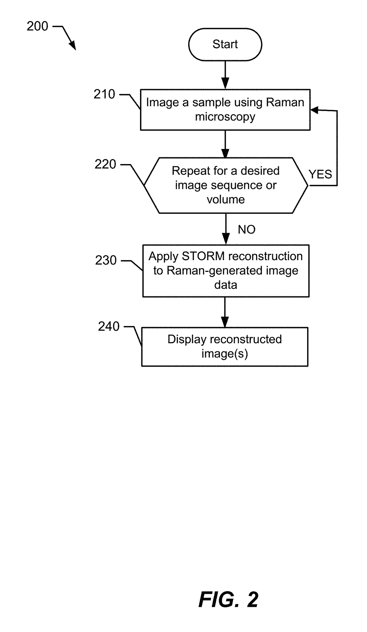
However, unlike STORM, a hybrid or modified STORM approach (e.g., Raman-STORM) relies on an intrinsic nature of materials and does not use contrast agents (e.g., fluorescents).
Rough or impure surfaces can lead to hot carrier degradation and shorter device lifetimes.
However, electron microscopy is expensive and large amounts of sample preparation are necessary using that technique.
Additionally, resolution of modified STORM imaging such as Raman-STORM imaging can rival the resolution of electron microscopes.
Lower resolution achieved through Raman imaging can be a problem when attempting to study small biological features that are beyond the resolution limit, such as mitochondria.
These disadvantages keep Raman microscopy from being highly employed in biological imaging.
Time is highly limited in data acquisition for techniques such as STED, PALM and STORM.
Furthermore, fluorescent dyes can perturb cell function with their cyto- and photo-toxicity.
This perturbation can affect cell function and interaction, making conclusive studies near impossible and skewing results.

Method used


Image

  • Devices, methods, and systems relating to super resolution imaging
  • Devices, methods, and systems relating to super resolution imaging
  • Devices, methods, and systems relating to super resolution imaging

Examples


example 1

[0193]As shown in FIG. 10a, a common lithographic polymer, PMMA was used to create a nanopattern sample on glass substrate, and then used the sample to confirm the source of the stochastic radiation. FIG. 10b shows a scanning electron microscopy (SEM) image of an “NU” logo pattern fabricated using E-Beam lithography with a 100 nm linewidth in a 200 nm-thick PMMA film. The 65 nm wide gap between the letters (highlighted in FIG. 10b) cannot be resolved using optical white-field microscopy (FIG. 10c), because the features size is well below the maximum diffraction-limited resolution of 225 nm using a 1.49-NA TIRF objective. A 532-nm laser was used to excite the sample, revealing stochastic radiation events. Images were reconstructed that localized stochastic radiation using STORM (FIG. 10d). Multiple locations of the glass substrate with and without PMMA coating were observed. Interestingly, stochastic blinking events were observed from the “NU” pattern (FIG. 10e) under modest laser po...

example 2

[0202]To determine the minimal resolvable feature size of our STORM setup using the intrinsic fluorescence from PMMA, the theoretically and experimentally resolution was calculated. Depending on detector parameters and filter efficiency, the theoretical resolution of STORM imaging can vary. If the probability of simultaneous stochastic light generation from multiple nearby regions is negligible, we can assume the detected PSFs to be from a single stochastic event. The center of the PSF can then be approximated with the probability equation,

σμi=(si2N)+(a2 / 12N)+(8πsi4b2a2N2)

where N is the number of detected photons; si is the standard deviation of the PSF; a is the pixel size; and b is the standard deviation of the background. As the number of detected photons determines the probabilistic center of the PSFs, resolution is limited by the photon count of the stochastic radiation, the detector background, and the efficiency of the optical setup. Using the probability equation and conside...

example 3

[0203]To experimentally verify the theoretical resolution, a new PMMA target was patterned with progressively increasing periodicity of 200 nm, 250 nm, 300 nm, and 400 nm for resolution tests (FIGS. 15a-e). SEM imaging was used to confirm periodicity and gap spacing, as shown in FIG. 15a. As expected, conventional wide-field imaging does not have the ability to resolve the line spacing of the PMMA periodic grating pattern (FIG. 15b). In order to determine the experimental resolution of intrinsic fluorescence using STORM, we collected 60,000 frames of images from both immersed and non-immersed nanostructures and performed STORM reconstruction. Conventional wide-field imaging and STORM images from non-immersed (FIG. 15c) and immersed (FIG. 15d) PMMA structures were averaged along the vertical axis to create line profiles of the intensity distribution (FIG. 15e). Clearly, patterns with periodicity of 200 nm can be well resolved for both PMMA nanopatterned samples, indicating a half-pit...


PUM

PropertyMeasurementUnit
wavelengthsaaaaaaaaaa

Abstract

Certain examples disclose systems and methods for imaging a target. An example method includes: a) activating a subset of light-emitting molecules in a wide field area of a target using an excitation light; b) capturing one or more images of the light emitted from the subset of the molecules illuminated with the excitation light; c) localizing one or more activated light emitting molecules using one or more single molecule microscopic methods to obtain localization information; d) simultaneously capturing spectral information for the same localized activated light emitting molecules using one or more spectroscopic methods; e) resolving one or more non-diffraction limited images of the area of the target using a combination of the localization and spectral information for the localized activated light emitting molecules; and 0 displaying the one or more non-diffraction limited images.

Description

RELATED APPLICATION[0001]This patent arises from the U.S. national stage of International Patent Application Serial No. PCT / US15 / 52388, having an International filing date of Sep. 25, 2015, and claims the benefit of U.S. Provisional Application Ser. No. 62 / 055,398, entitled “Intrinsic-Contrast Super-Resolution Optical Microscope,” which was filed on Sep. 25, 2014, both of which are hereby incorporated herein by reference in their entireties.STATEMENT REGARDING FEDERALLY SPONSORED RESEARCH OR DEVELOPMENT[0002]This invention was made with government support under grant numbers R01EY019951, R24EY022883, and R01CA165309 awarded by the National Institutes of Health; and grant numbers DBI-1353952, CBET-1055379, CBET-1066776, EFRI-1240416, and CMMI-0955195 awarded by the National Science Foundation. The government has certain rights in the invention.FIELD OF THE DISCLOSURE[0003]This disclosure relates generally to characterizing biological tissue and material and, more particularly, to cha...

Claims


Application Information

Patent Timeline
Patent Type & Authority Applications(United States)
IPC IPC(8): G01J1/42G01N33/483G01N21/84
CPCG01J1/4228G01N33/483G01N21/84G02B21/0076G01N21/6458G01N21/65G02B21/0032G02B21/0064G02B21/008G02B21/367G02B27/58
Inventor URBAN, BENZHANG, HAO F.SUN, CHENGDONG, BIQIN
Owner NORTHWESTERN UNIV
Learn More