
Complex circuit, circuit device, circuit board, and communication device

Active Publication Date: 2017-06-15
TAIYO YUDEN KK
View PDF13 Cites 6 Cited by
  • Summary
  • Abstract
  • Description
  • Claims
  • Application Information

AI Technical Summary

Benefits of technology

The present invention allows for the creation of complex electronic circuits, devices, and boards that can support a wider range of frequencies. This results in improved performance and increased flexibility for use in communication devices.

Problems solved by technology

Baluns convert balanced signals to unbalanced signals or convert unbalanced signals to balanced signals.

Method used


Image

  • Complex circuit, circuit device, circuit board, and communication device
  • Complex circuit, circuit device, circuit board, and communication device
  • Complex circuit, circuit device, circuit board, and communication device

Examples


modification examples

6. Other Embodiments and Modification Examples

[0130]The present invention is not limited to the embodiments described above and can be implemented in the form of various other embodiments.

[0131]In the embodiments described above, the inductor electrodes 71, 72, 73, and 74 are formed in coil shapes and only on top of the dielectric sheet 105. However, in order to achieve higher inductance values, the inductor electrodes may be formed in spiral shapes spanning a plurality of dielectric sheets (here, “spiral-shaped” refers to a three-dimensional shape that extends in the layering direction). This configuration also makes it possible to achieve the same effects as in the embodiments described above. Moreover, the inductor electrodes may also be formed as two-layer structures in order to decrease the conductivity thereof and thereby improve the Q factors of the resulting inductors.

[0132]In the diplexer 20, the orders (numbers of stages) of the low-pass filters 21 and the high-pass filter...


PUM


Abstract

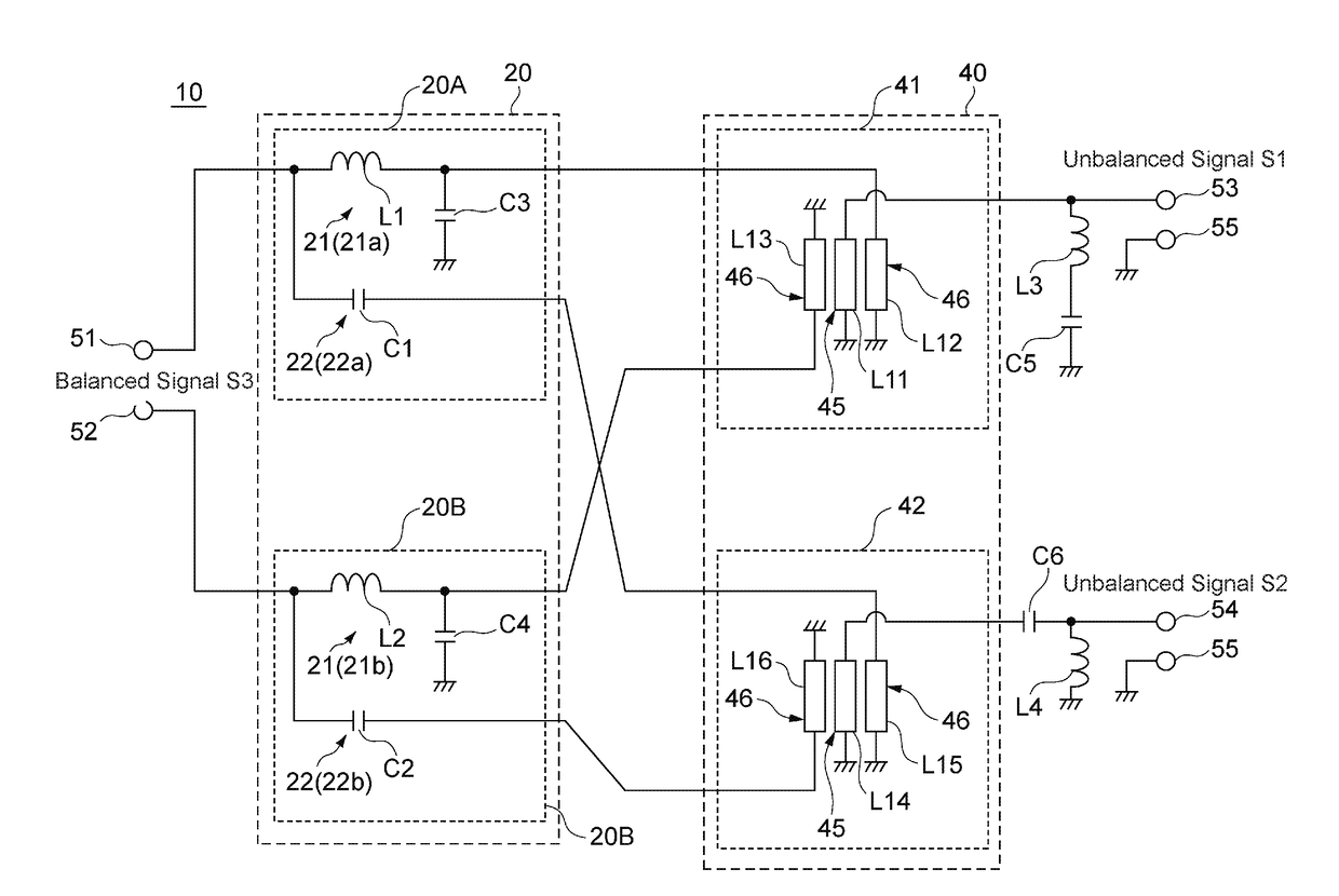
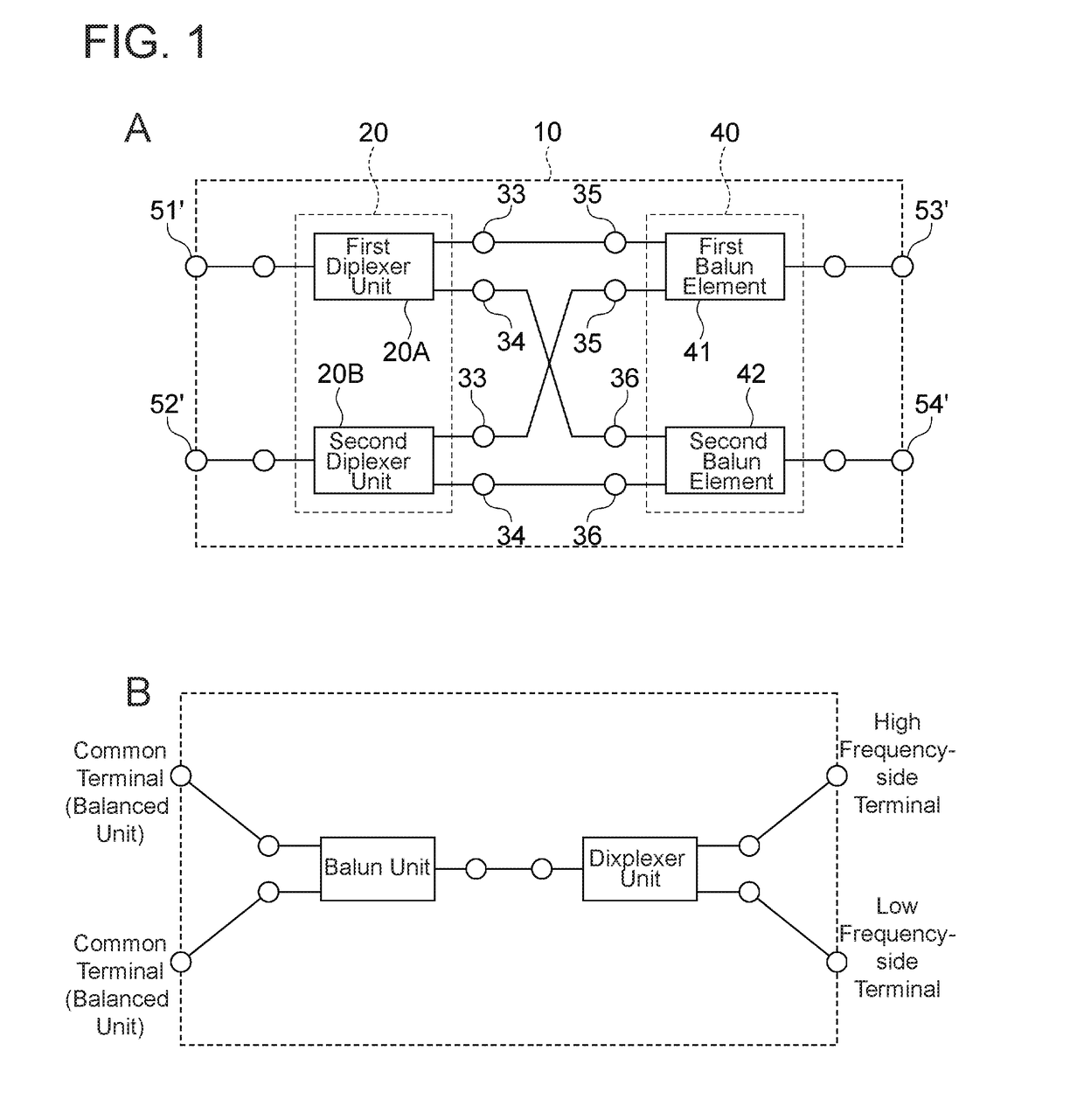
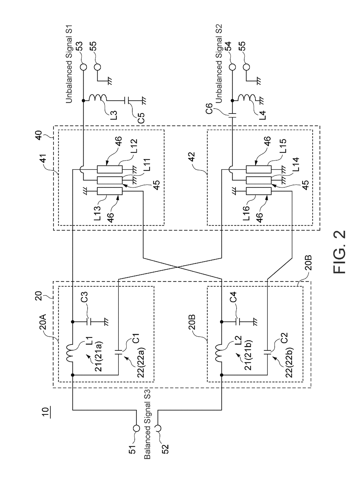
PROBLEM: To provide a high-performance complex circuit, circuit device, circuit board, and communication device that support a wider band of frequencies.SOLUTION: A complex circuit includes a first diplexer that passes through the normal-phase signals of balanced signals and a second diplexer that passes through the reverse-phase signals of the balanced signals. A balun includes a low frequency band first balun element and a high frequency band second balun element. The first balun element and the second balun element respectively include a plurality of lines that are connected to the first diplexer and that carry signals occupying two different frequency bands and also respectively include a plurality of lines that are connected to the second diplexer and that carry signals occupying two different frequency bands. The lines form one pair of balanced lines, and the lines form another pair of balanced lines. Furthermore, the first balun element and the second balun element each include an unbalanced line.

Description

TECHNICAL FIELD[0001]The present invention relates to a technology such as a complex circuit for removing unnecessary interfering waves or for multiplexing and demultiplexing a plurality of signals. Typically, the present invention relates to a technology for use in wireless communication devices that can communicate using the Long-Term Evolution (LTE) wireless communication standard.[0002]Here, “interfering waves” refers to unwanted signals outside of the desired frequency band, such as wireless signals sent from another transmitter, wireless signals sent from a transceiver, or unwanted electromagnetic radiation from another integrated circuit (IC), for example.BACKGROUND ART[0003]Wireless communication devices such as smartphones are being used on an increasingly global basis, and devices that can be used in multiple countries are in demand. In recent years, for example, communication systems such as LTE have begun to be introduced in many countries. However, in many cases the fre...

Claims


Application Information

Patent Timeline
IPC IPC(8): H03H7/46H03H7/01H04B1/40H03H7/42
CPCH03H7/46H04B1/40H03H7/0115H03H7/42H01F19/06H01P5/10H01F17/0006H01F17/0013H01P1/2135H04B1/0057H01F2017/0066H01F2017/0073H03H2001/0085
Inventor SAITO, TOSHIYUKI
Owner TAIYO YUDEN KK
Learn More