
Printable Films for Printed Circuit Boards and Processes for Making Same

a technology of printed circuit boards and printed circuit boards, applied in the direction of printed circuit parts, printed circuit dielectrics, transparent dielectrics, etc., can solve the problems of requiring significant equipment and potentially hazardous materials, requiring days or weeks to complete, and presently cumbersome construction of physical electronics prototypes

Inactive Publication Date: 2017-05-11
ADDEM LABS INC
View PDF1 Cites 4 Cited by
  • Summary
  • Abstract
  • Description
  • Claims
  • Application Information

AI Technical Summary

Benefits of technology

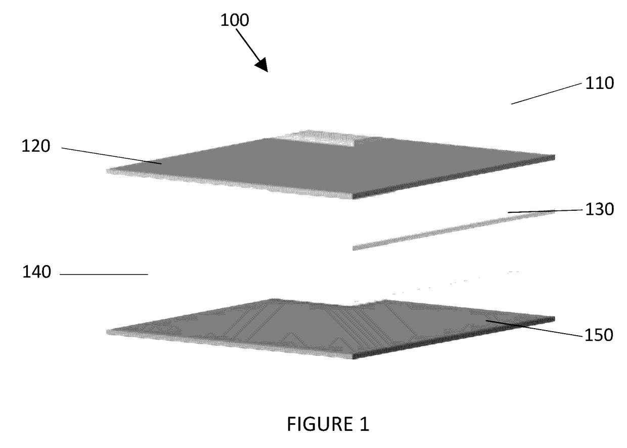
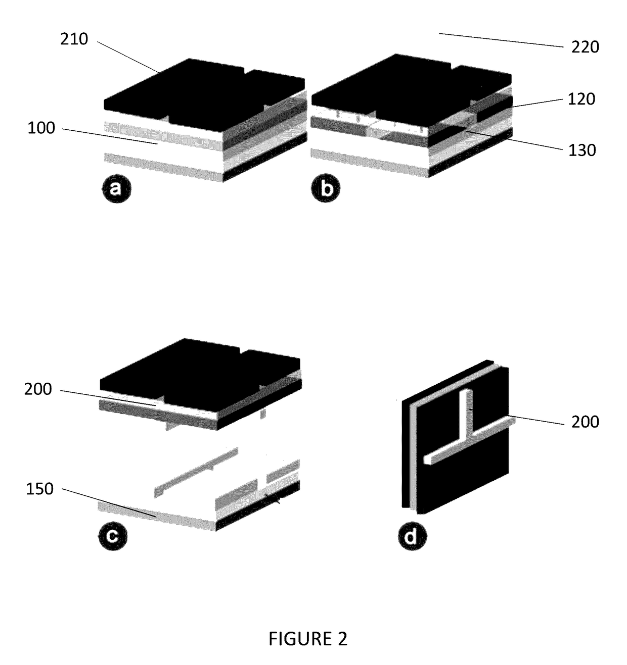
This patent describes a printable film that can be used to make printed circuit boards. The film has three layers: a first layer that is transparent to radiation, a second layer that is made of a curable adhesive that can be cured by exposing it to radiation, and a third layer that is made of a conductive material. The film can be inked with a pattern that represents the circuit board, and then exposed to radiation to cure the adhesive and remove parts of the conductive material to form the final circuit board. The film can be used to simplify the production of printed circuit boards and make them more efficient.

Problems solved by technology

Despite their prominence, building physical electronics prototypes is presently cumbersome.
Industrial processes, such chemical etching, require significant equipment and potentially hazardous materials, and may take days or weeks to complete.
Rapid prototyping methods such as silver inks are expensive and require special equipment.
Without the ability to effectively fabricate PCBs quickly, users cannot rapidly build and iterate on the design and development of physical objects that possess computational abilities, or the degree of “smartness” necessary, to sense the environment, interact with users, or communicate with the digital world.

Method used


Image

  • Printable Films for Printed Circuit Boards and Processes for Making Same
  • Printable Films for Printed Circuit Boards and Processes for Making Same
  • Printable Films for Printed Circuit Boards and Processes for Making Same

Examples


example 1

Shield

[0091]To demonstrate the quick prototyping use of PCB film, a simple LED bar graph shield for the Arduino Uno™ may be built. Due to the simplicity and rapidity of using PCB film 100, such ad hoc circuits may be tested quickly and then cut into a variety of shapes for later use.

[0092]FIGS. 3A and 3B show the Arduino™ shield 300. As shown in FIG. 3A, the attachment points 310 for the Arduino™ pin-outs are on the right side of the PCB, and the leads and mount points 320 for each LED in the array are in the center, along with the leads and mount points for a single resistor beneath the array. FIG. 3B shows the working PCB 300, where the Arduino Uno 330™ is controlling the LED array 340. In this example, the PCB was printed in several seconds, plus an additional two minutes to cure. Components were then attached using a stencil, as described above. Also, while the PCB is generally flexible, this device is better provided with rigidity. To this end, the PCB was affixed to a rigid su...

example 2

mb

[0093]As shown in FIGS. 4A and 4B, this device 400 indicates when a plant needs to be watered. The circuit consists of an Attiny85™ microcontroller 410 that repeatedly measures the resistance of the soil, triggering a red LED 420 whenever the moisture falls below a certain threshold set using the onboard potentiometer 430. For assembly, the components have been affixed to the PCB using conductive epoxy as shown in FIG. 4A, but without the use of a mask, after making holes in the PCB at the right places, the components are inserted through and the conductive epoxy is applied. Finally, scissors are used to cut the PCB to the desired shape.

example 3

Shortcut Pad

[0094]As shown in FIGS. 5A and 5B, the flexibility of PCB film 100 may be leveraged to create objects with interesting shapes, using the PCB film 100 to create componentry, rather than simply the traditional elements of a PCB. In this case, a simple user interface device: a shortcut pad 500 that triggers various shortcuts in OSX. An Arduino Pro Micro™510 has been combined with a simple capacitive sensing technique to create a touchpad 520. The circuit triggers a keyboard command through the USB whenever the touchpad 520 on the PCB is touched. The physical substrate was created using a laser-cut acrylic that was reshaped with a heat-gun, onto which the PCB was mounted. As shown in FIG. 5B, the PCB is then adhered to a bent acrylic mounting.

[0095]Naturally, traditional buttons could have been mounted onto the PCB if desired. However, the use of the PCB film 100 to create the input pad itself demonstrates the sort of flexible prototyping that the PCB film 100 affords. Also,...


PUM


Abstract

Film for use in preparing a printed circuit board (PCB) along with methods for making a PCB and producing a printable film are described herein. The film includes a first layer formed of a radiation-transparent material, a second layer formed of a curable adhesive material, a third layer formed of an electrically conductive material, and optionally, a fourth layer formed of an adhesive and a fifth layer formed of a removable material. Through the adhesive layers, the layers are bonded together to produce the printable film. To produce a PCB, the first layer is covered in ink distributed in a pattern representing the PCB, and the ink-covered film is exposed to radiation until the non-ink-covered portions of the second layer have cured. Then, the fifth layer is removed tearing away the electrically conductive material associated with the non-ink-covered portions of the second layer producing the PCB.

Description

FIELD OF THE INVENTION[0001]The present specification relates generally to the fabrication of Printed Circuit Boards (PCBs), and more specifically to printable films and methods that allow end users to make PCBs that are possible using standard office inkjet or laser printers, using standard inks.BACKGROUND OF THE INVENTION[0002]Printed Circuit Boards (PCBs) form the structural and connective underpinnings of electronic assemblies. Nearly every electronic device contains one or more PCBs on which the functional components such as integrated circuits (ICs), resistors and other passive components, connectors, etc. are placed. PCBs function to provide power to the various components, enable communication, and act as a mechanical support structure to allow the assembly to be fixed into enclosures.[0003]Despite their prominence, building physical electronics prototypes is presently cumbersome. Industrial processes, such chemical etching, require significant equipment and potentially haza...

Claims


Application Information

Patent Timeline
Patent Type & Authority Applications(United States)
IPC IPC(8): H05K3/02H05K1/09
CPCH05K3/027H05K1/092H05K2203/068H05K2201/0335H05K2201/032H05K2203/013H05K2203/0525H05K2203/0551H05K3/048H05K2203/0264H05K3/06H05K2201/0108H05K2201/0355H05K3/04H05K1/0386
Inventor CHADALAVADA, PERUMAL VARUNWIGDOR, DANIEL
Owner ADDEM LABS INC
Learn More