Pixel of an organic light emitting diode display device and organic light emitting diode display device

a technology of light emitting diodes and display devices, which is applied in the direction of semiconductor devices, instruments, electrical apparatuses, etc., can solve the problems of increasing accelerating the degradation of the driving transistor, and worsening of unwanted threshold voltage compensation voltage changes, etc., to achieve the effect of improving the luminance uniformity of the organic light emitting diode display device and reducing the stress applied to the driving transistor

Active Publication Date: 2017-05-04
SAMSUNG DISPLAY CO LTD
View PDF3 Cites 33 Cited by
  • Summary
  • Abstract
  • Description
  • Claims
  • Application Information

AI Technical Summary

Benefits of technology

[0008]Some example embodiments provide a pixel of an organic light emitting diode display device capable of reducing a stress applied to a driving transistor, accurately compensating a threshold voltage of the driving transistor, and maintaining a voltage of an anode of an organic light emitting diode to be substantially constant until the organic light emitting diode emits light.
[0009]Some example embodiments provide an organic light emitting diode display device capable of reducing a stress applied to a driving transistor, accurately compensating a threshold voltage of the driving transistor, and maintaining a voltage of an anode of an organic light emitting diode to be substantially constant until the organic light emitting diode emits light.
[0030]As described above, in the pixel of the organic light emitting diode display device and in the organic light emitting diode display device according to example embodiments, because the driving transistor is initialized to the off-bias state, the stress applied to the driving transistor may be reduced.
[0031]In addition, in the pixel of the organic light emitting diode display device and in the organic light emitting diode display device according to example embodiments, a voltage of a gate of the driving transistor may be initialized to a substantially fixed voltage before a threshold voltage compensation operation for the driving transistor is initiated, and thus an initial voltage level of the threshold voltage compensation voltage provided to the compensation capacitor may not be undesirably changed over time. Accordingly, the threshold voltage of the driving transistor may be accurately compensated even after the lapse of time.
[0032]Further, in the pixel of the organic light emitting diode display device and in the organic light emitting diode display device according to example embodiments, a voltage of an anode of the organic light emitting diode may be maintained to be substantially constant and to be substantially uniform with respect to all of the pixels until the organic light emitting diode emits light, and thus luminance uniformity of the organic light emitting diode display device may be improved.

Problems solved by technology

However, in this case, because the driving transistors are turned on in each and every frame, degradation of the driving transistors may be accelerated.
This unwanted threshold voltage compensation voltage change may be worsened by a characteristic change of the parasitic capacitor of the OLED caused by degradation of the OLED.
Further, this unwanted voltage change may further be worsened when an anode of the OLED is sufficiently initialized.

Method used


Image

  • Pixel of an organic light emitting diode display device and organic light emitting diode display device
  • Pixel of an organic light emitting diode display device and organic light emitting diode display device
  • Pixel of an organic light emitting diode display device and organic light emitting diode display device

Examples


Embodiment Construction

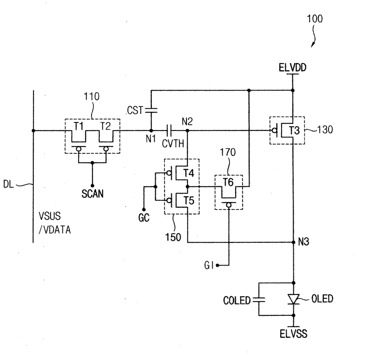
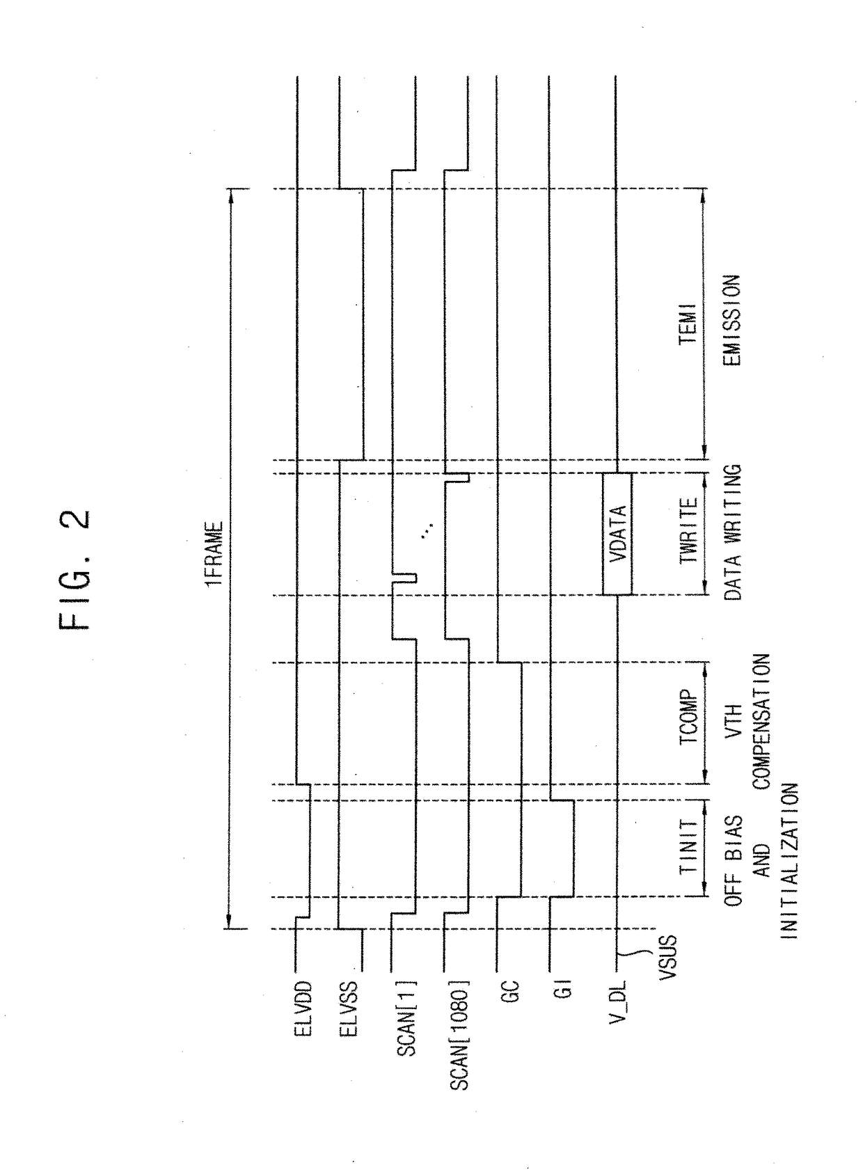
[0061]The example embodiments are described more fully hereinafter with reference to the accompanying drawings. Like or similar reference numerals refer to like or similar elements throughout.

[0062]It will be understood that, although the terms “first,”“second,”“third,” etc., may be used herein to describe various elements, components, regions, layers, and / or sections, these elements, components, regions, layers, and / or sections should not be limited by these terms. These terms are used to distinguish one element, component, region, layer, or section from another element, component, region, layer, or section. Thus, a first element, component, region, layer, or section discussed below could be termed a second element, component, region, layer, or section, without departing from the spirit and scope of the present invention.

[0063]Further, it will also be understood that when one element, component, region, layer, and / or section is referred to as being “between” two elements, component...


PUM


Abstract

A pixel of an organic light emitting diode display device includes a scan transistor configured to connect a data line to a first node in response to a scan signal, a storage capacitor connected between the first node and a first power supply voltage, a compensation capacitor connected between the first node and a second node, a driving transistor having a gate connected to the second node, a source connected to the first power supply voltage, and a drain connected to a third node, a compensation transistor configured to connect the second node to the third node in response to a compensation control signal, an organic light emitting diode connected between the third node and a second power supply voltage, and an initialization transistor configured to transfer an initialization voltage in response to an initialization control signal.

Description

CROSS-REFERENCE TO RELATED APPLICATION[0001]This application claims priority to and the benefit of Korean Patent Application No. 10-2015-0150483, filed on Oct. 28, 2015 in the Korean Intellectual Property Office (KIPO), the content of which is incorporated herein in its entirety by reference.BACKGROUND[0002]1. Field[0003]Example embodiments relate to pixels of organic light emitting diode (OLED) display devices and the OLED display devices.[0004]2. Description of the Related Art[0005]In an organic light emitting diode (OLED) display device, a driving transistor included in each pixel generates a driving current based on a data voltage applied to the pixel, and an OLED included in the pixel emits light, based on the driving current, to display an image.[0006]The driving transistor may have a hysteresis characteristic such that a characteristic curve of the driving transistor in a current frame is changed according to an operating state of the driving transistor in a previous frame. T...

Claims


Application Information

Patent Timeline
Patent Type & Authority Applications(United States)
IPC IPC(8): G09G3/3258H01L27/32
CPCG09G3/3258G09G2310/08G09G2330/00H01L27/3244G09G3/3233G09G2300/0819G09G2300/0852G09G2300/0861G09G2300/0866G09G2320/045H10K59/12
Inventor PARK, KYONG-TAECHO, KYU-SIKLEE, JIN-A
Owner SAMSUNG DISPLAY CO LTD
Why Eureka
Try Eureka