Photosensitive laminate, transfer material, patterned photosensitive laminate, method for manufacturing the same, touch panel, and image display device
- Summary
- Abstract
- Description
- Claims
- Application Information
AI Technical Summary
Benefits of technology
Problems solved by technology
Method used
Image
Examples
first embodiment
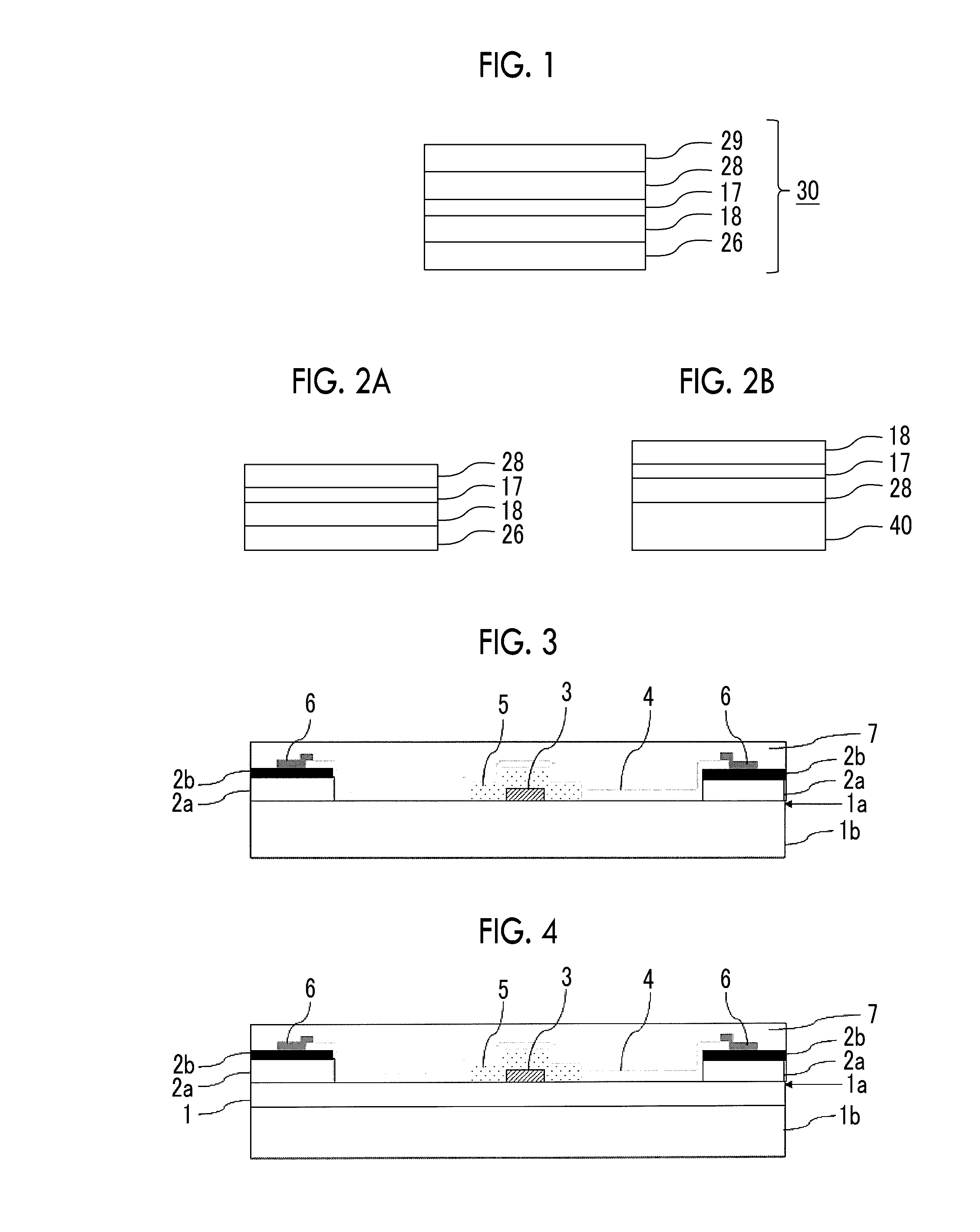
[0193]First, a configuration of the touch panel according to the first embodiment that is formed by the manufacturing method according to the invention is described. FIGS. 3 and 4 are sectional views illustrating a preferable configuration in the touch panel according to the first embodiment of the invention. The touch panel in FIG. 3 includes a front surface plate 1b (cover glass), a white coloration layer (first resin layer) 2a, a light shielding layer (second resin layer) 2b, a first transparent electrode pattern 3, a second transparent electrode pattern 4, an insulating layer 5, a conductive element 6, and a transparent protective layer 7. The touch panel includes an interlayer (not illustrated) between the white coloration layer 2a and the light shielding layer 2b.
[0194]The front surface plate 1 and / or 1b is preferably formed with light transmissive substrates. As the light transmissive substrate, any one of a substrate provided with the decorative material on the cover glass ...
second embodiment
[0205]The preferable configuration of the touch panel according to the second embodiment of the invention is described together with the method for manufacturing respective members forming the device. The descriptions of portions that are overlapped with those in the first embodiment are appropriately omitted.
[0206]FIG. 12 is a sectional view schematically illustrating a preferable configuration of the touch panel according to the second embodiment the invention. In FIG. 12, an embodiment in which a touch panel 10 according to the second embodiment is formed with the transparent substrate (front surface plate) 1, the decorative material 2, a transparent film 11 having a refractive index of 1.6 to 1.78 and a film thickness of 55 nm to 110 nm, the first transparent electrode patterns 3, the second transparent electrode patterns 4, the insulating layer 5, the conductive elements 6, a second curable transparent resin layer (refractive index adjusting layer) 12, and a first curable trans...
example 1
Manufacturing of Transfer Material
[0215]>
[0216]As a temporary support, a surface of a release layer of a polyethylene terephthalate (PET) base (UNIPEEL TR6, manufactured by Unitika Ltd., and thickness of 50 μm) with a release layer was coated with a second resin layer coating liquid (K1) consisting of prescription below, and drying was performed at 120° C. for 2 minutes, so as to obtain a second resin layer (light shielding layer) having a dry film thickness of 3 μm.
[0217](Coating Liquid for Second Resin Layer: Prescription K1)
Carbon black dispersion liquid (Pigment ratio: 360 parts by mass31.3%, composition below):Propylene glycol monomethyl ether acetate: 115 parts by massMethyl ethyl ketone: 400 parts by massPhotopolymerization initiator (IRGACURE 907,2.38 parts by massmanufactured by BASF Japan Ltd.):Acryl-based resin in structure represented in61.1 parts by mass[Chem. 1] below:Monomer DPHA (propylene glycol monomethyl61.2 parts by massether acetate solution solid content: 76 ma...
PUM
 Abstract
Description
Claims
Application Information
 - R&D
- Intellectual Property
- Life Sciences
- Materials
- Tech Scout
- Unparalleled Data Quality
- Higher Quality Content
- 60% Fewer Hallucinations
Browse by: Latest US Patents, China's latest patents, Technical Efficacy Thesaurus, Application Domain, Technology Topic, Popular Technical Reports.
© 2025 PatSnap. All rights reserved.Legal|Privacy policy|Modern Slavery Act Transparency Statement|Sitemap|About US| Contact US: help@patsnap.com


