
Processes for using flux agents to form polycrystalline group iii-group v compounds from single source organometallic precursors

a technology of polycrystalline group iii-group v and flux agent, which is applied in the direction of arsenic compounds, liquid/solution decomposition chemical coatings, electrically-conductive paints, etc., can solve the problems of large grains of stoichiometric gaas, significant problem, waste of mocvd process, etc., and achieves better electronic properties and increase the size of crystalline grains

Inactive Publication Date: 2016-11-03
DOW GLOBAL TECH LLC
View PDF0 Cites 4 Cited by
  • Summary
  • Abstract
  • Description
  • Claims
  • Application Information

AI Technical Summary

Benefits of technology

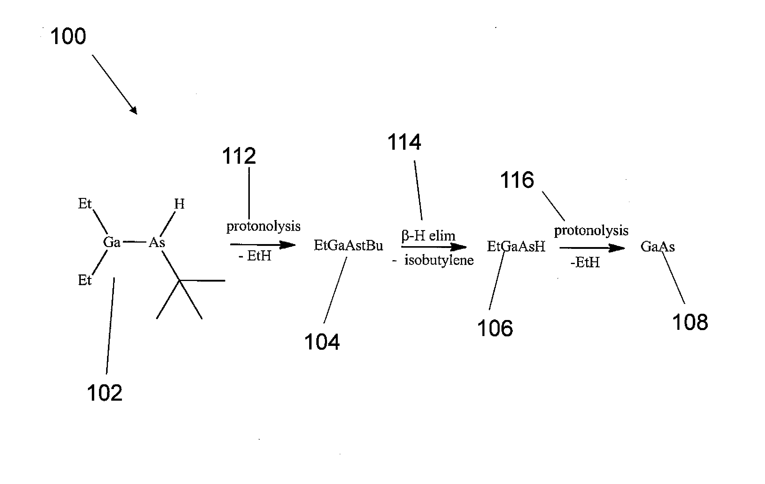
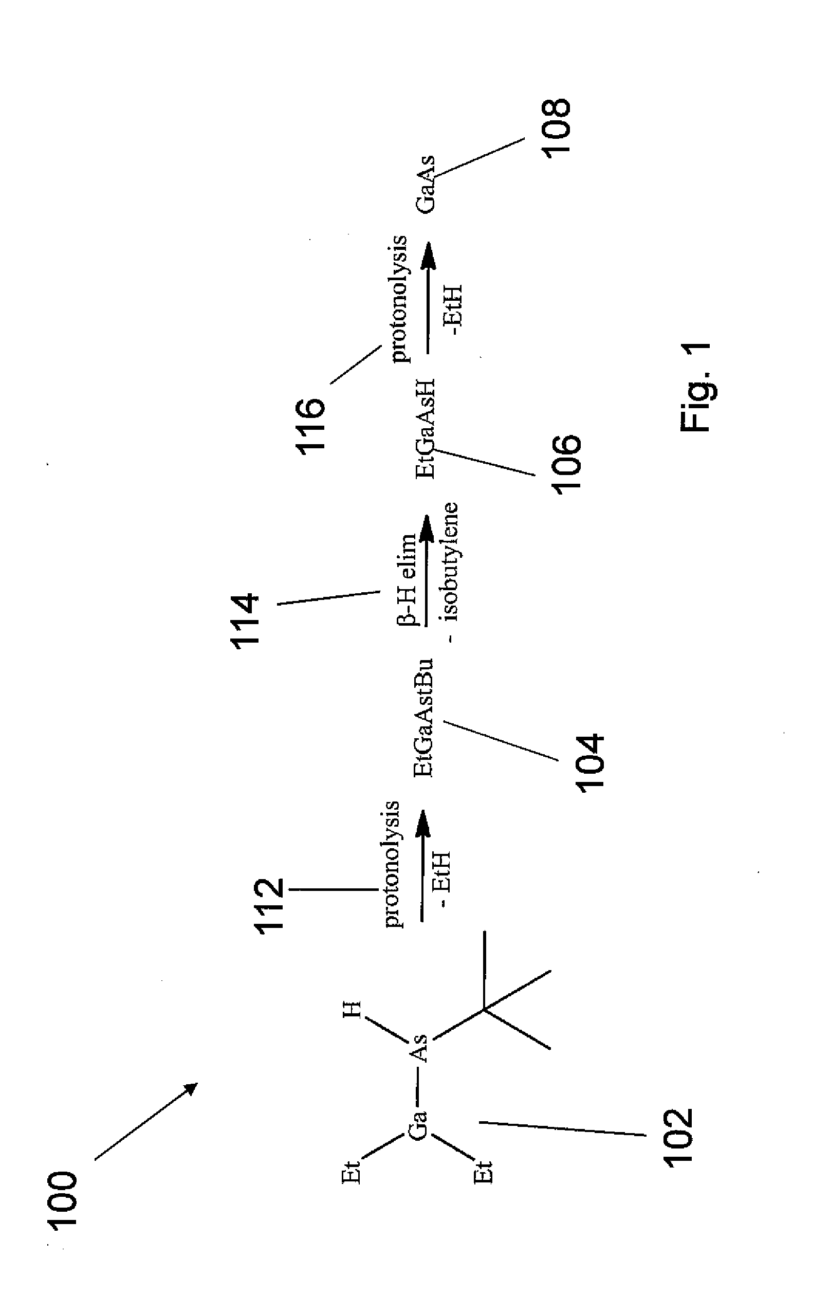
The present invention provides better methods for making certain semiconductor compounds using single source organometallic precursors. This can help control the stoichiometry, or ratios, of the elements in the compounds. The invention also suggests annealing the precursors in the presence of flux agents to increase the size of the crystal grains in the semiconductor compounds. This can improve the electronic properties of the semiconductors. The flux layer may also help control the stoichiometry of the compounds.

Problems solved by technology

Unfortunately, MOCVD provides large grains of stoichiometric GaAs at the expense of Ga and As utilization.
This is a significant problem.
Therefore, the MOCVD process is wasteful, and Ga and As materials are very expensive.
This expense in combination with inefficient utilization is one of the main reasons that GaAs solar cells are not cost competitive with other technologies.
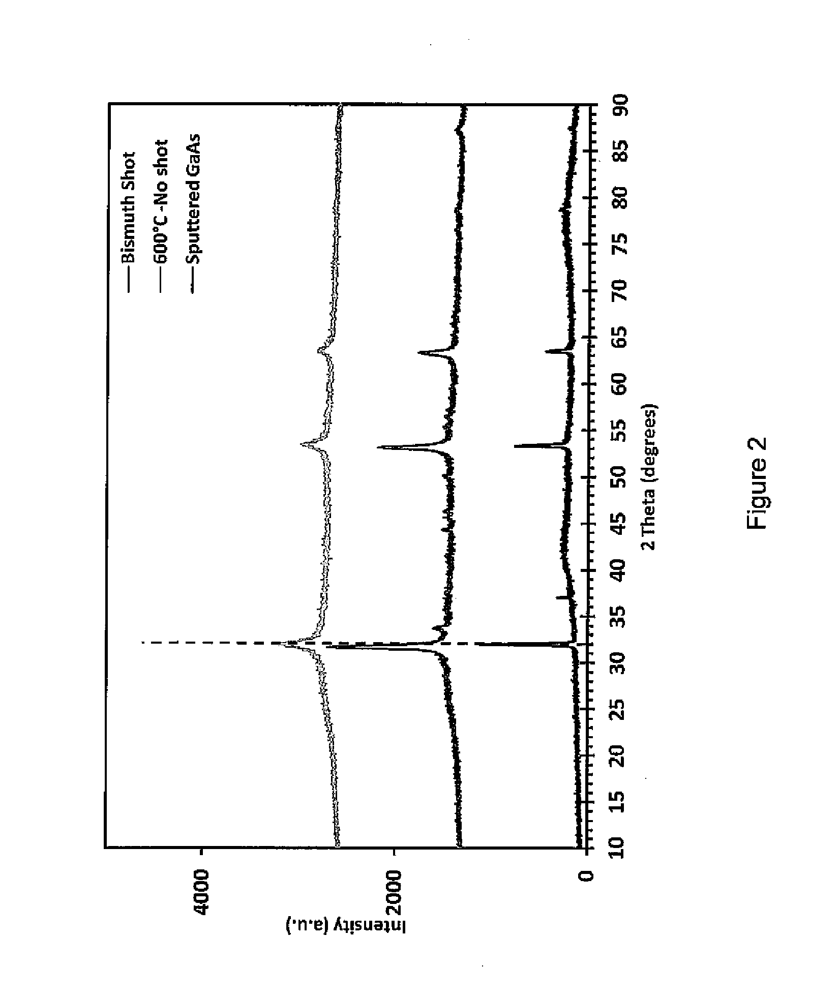
As one significant challenge, our XRD analysis of GaAs fabricated from previously known methods using single source organometallic precursors indicates that the resultant GaAs has relatively small crystalline grains and might not even be fully polycrystalline.
This is particularly problematic when those precursors are coated onto a substrate in the liquid phase using solution deposition or the like.
The small crystalline grains undermines electronic performance in many applications.
As another challenge, our EDS analysis of GaAs fabricated from previously known methods using single source organometallic precursors indicates that the resultant GaAs is not stoichiometric and may have a Ga and As content that differs substantially from that of the single source precursor.
The stoichiometric deficiency is particularly problematic when those precursors are coated onto a substrate in the liquid phase using solution deposition or the like.
However, annealing the precursor may tend to produce polycrystalline gallium arsenide that is significantly deficient with respect to gallium and / or arsenic.
In some uses, this deficiency is problematic.
Loss of gallium and / or arsenic reduces the efficiency by which the single source precursor is used to form the desired polycrystalline GaAs product.

Method used


Image

  • Processes for using flux agents to form polycrystalline group iii-group v compounds from single source organometallic precursors
  • Processes for using flux agents to form polycrystalline group iii-group v compounds from single source organometallic precursors
  • Processes for using flux agents to form polycrystalline group iii-group v compounds from single source organometallic precursors

Examples


example 1

Synthesis of [tBu(H)AsGaMe2]n

[0079]A 40 mL vial was charged with tBuAsH2 (134 mg, 1 mmol) and diluted with hexane (15 mL). To the vial, Me3Ga (1 mmol, 115 mg) was added. The mixture was heated to about 70° C. for 24 h. The volatiles were removed under reduced pressure to afford a colorless solid Yield: 211 mg, 90.6%. 1H NMR (400 MHz, C6D6, 25° C.): δ 2.37, (s, As—H, 0.22H), 2.25 (s, As—H, 0.42H), 2.08 (s, As—H, 0.22H), 1.30 (m, As-tBu, 9H), 0.36 (s, Ga-Me, 1.28H), 0.33 (s, Ga-Me, 1.15H), 0.31 (s, Ga-Me, 1.87H), 0.28 (s, Ga-Me, 0.71H). 13C NMR (101 MHz, C6D6, 25° C.): δ 35.75, 35.38, 35.07, 34.07, 33.77, 1.24, 0.45, −1.28, −1.59, −3.10, −3.29.

example 2

Synthesis of [tBu(H)AsGaEt2]n

[0080]A 40 mL vial was charged with tBuAsH2 (134 mg, 1 mmol) and diluted with hexane (15 mL). To the vial, Et3Ga (1 mmol, 156 mg) was added. The mixture was heated to about 70° C. for 24 h. The volatiles were removed under reduced pressure to afford a colorless solid. Yield: 238 mg, 91.5%. 1H NMR (400 MHz, C6D6, 25° C.): δ 2.39, (s, As—H, 0.27H), 2.30 (s, As—H, 0.52H), 2.17 (s, As—H, 0.14H), 1.43 (m, Ga—CH2CH3, 6H), 1.35 (m, As-tBu, 9H), 0.93 (M, Ga—CH2CH3, 4 H). 13C NMR (101 MHz, C6D6, 25° C. 13C NMR) 8 35.40, 35.11, 34.89, 34.36, 34.17, 12.67, 12.52, 12.30, 12.14, 11.81, 11.68, 9.15, 8.63, 8.24, 8.08, 7.38, 7.08.

example 3

Synthesis of {[tBu(H)AsGaEt2]3(tBuAsGaEt)2}

[0081]A 5 mL vial was charged with tBuHAsGaEt2 (0.242 g, 0.9272 mmol) and dissolved in hexane (1 mL). The solution was stored in the dry box for 53 days and it was noticed that colorless crystals appeared. Yield (19%; 44 mg). The crystals were shown to be {[tBuAs(H)GaEt2]3(tBuAsGaEt)2} by X-ray crystallography and NMR spectroscopy. 1H NMR (400 MHz, C6D6, 25° C.): δ 2.9, (s, As—H, 1.03H), 2.87 (s, As—H, 1.00H), 2.55 (s, As—H, 1.05H), 1.50 (m, Ga—CH2CH3, 18H and As-tBu, 18H), 1.38-1.25 (m, Ga—CH2CH3, 6H), 1.38 (s, As-tBu, 9H), 1.35 (s, As-tBu, 9H), 1.27 (s, As-tBu, 9H), 1.25-0.95 (m, Ga—CH2CH3, 16 H).


PUM

PropertyMeasurementUnit
pressureaaaaaaaaaa
boiling pointaaaaaaaaaa
melting pointaaaaaaaaaa

Abstract

The present invention provides methods for using single source organometallic precursors in the fabrication of polycrystalline Group III-Group V compounds, preferably semiconductor compounds. The present invention teaches how to select organometallic ligands in single-source precursors in order to control the stoichiometry of the corresponding Group III-Group V compounds derived from these precursors. The present invention further teaches how to anneal precursors in the presence of one or more flux agents in order to increase the crystalline grain size of polycrystalline Group III-Group V compounds derived from organometallic precursors. This helps to provide Group III-Group V semiconductors with better electronic properties. The flux layer also helps to control the stoichiometry of the Group III-Group V compounds.

Description

CROSS-REFERENCE TO RELATED APPLICATIONS[0001]This application claims priority to U.S. Provisional Patent Application No. 61 / 921,840, filed Dec. 30, 2013, the entire contents of which are incorporated herein by reference in its entirety.FIELD OF THE INVENTION[0002]The present invention relates to forming polycrystalline Group III-Group V compounds (e.g., polycrystalline gallium arsenide) from organometallic precursors. More particularly, the present invention relates to forming polycrystalline Group III-Group V pnictides (e.g., polycrystalline gallium arsenide) from organometallic precursors, wherein the precursors are annealed in the presence of one or more flux agents in order to provide polycrystalline Group III-Group V compounds with improved crystallinity and electronic characteristics.BACKGROUND OF THE INVENTION[0003]Solar cells are microelectronic devices that convert solar radiation and other light into usable electrical energy. The energy conversion occurs as the result of t...

Claims


Application Information

Patent Timeline
Patent Type & Authority Applications(United States)
IPC IPC(8): H01L21/02H01L31/18C07F9/74H01L21/324C09D5/24C07F9/72
CPCH01L21/02546C09D5/24C07F9/72H01L31/184H01L21/02628H01L21/3245H01L21/02595C07F9/743C01G28/00C07F19/00C23C18/1204C23C18/1275C07F9/74H01L21/02538Y02E10/544
Inventor WRIGHT, ROBERT J.SOKOLOV, ANATOLIY N.ATHENS, GEORGE L.NICKIAS, PETER N.STEVENS, JAMES C.SPENCER, LIAM L.GERHART, BRUCE B.PICKENS, ANNA M.
Owner DOW GLOBAL TECH LLC
Learn More