Touch panel and method for driving the same, and touch display device

a touch display device and touch panel technology, applied in the field of liquid crystal display technologies, can solve the problems of touch crosstalk and reduce the signal to noise ratio of the touch panel, and achieve the effect of improving the signal to noise ratio and improving the touch crosstalk

Active Publication Date: 2016-10-06
SHANGHAI TIANMA MICRO ELECTRONICS CO LTD +1
View PDF7 Cites 8 Cited by
  • Summary
  • Abstract
  • Description
  • Claims
  • Application Information

AI Technical Summary

Benefits of technology

[0016]In the touch panel according to embodiments of the disclosure, the first touch electrode line is configured to transmit a touch detection signal to the first touch electrode, and the first touch electrode line is disposed at a position where the first touch electrode line does not overlap with a projection region of other touch electrode driven simultaneously with the first touch electrode in a direction perpendicular to the touch panel. That is, there is no overlapping area for the first touch electrode and the touch electrode driven simultaneously with the first electrode. In this way in a case that the first touch electrode is driven, no parasitic capacitance is generated between the first touch electrode line and the touch electrode driven simultaneously with the first touch electrode. In this way, compared with the conventional solution in which driving each touch electrode results in generation of parasitic capacitance, in driving the touch panel according to the disclosure, less parasitic capacitance is generated, touch crosstalk is improved and the signal to noise ratio is increased.

Problems solved by technology

A touch electrode line connected to a driven touch electrode passes by other touch electrodes, and the other touch electrodes are also driven, in this way a parasitic capacitance is generated between the touch electrode line and the other touch electrodes, which causes touch crosstalk and decreases a signal to noise ratio of the touch panel.

Method used


Image

  • Touch panel and method for driving the same, and touch display device
  • Touch panel and method for driving the same, and touch display device
  • Touch panel and method for driving the same, and touch display device

Examples


first embodiment

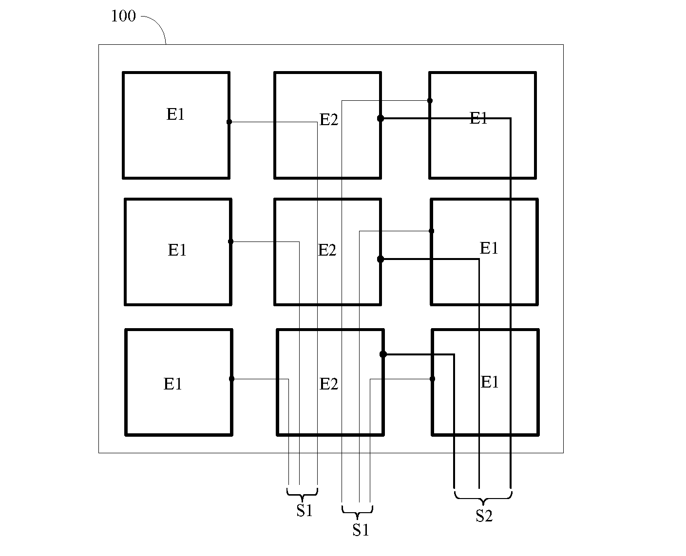
[0027]FIG. 1 is a schematic structural diagram of a touch panel according to the disclosure. As shown in FIG. 1, the touch panel includes a substrate 100 and multiple touch electrodes and multiple touch electrode lines located on the substrate 100, where each touch electrode is electrically connected to a respective touch electrode line.

[0028]In the touch panel according to the disclosure, the touch electrodes include first touch electrodes E1 and second touch electrodes E2. The touch electrode lines include first touch electrode lines S1 and second touch electrode lines S2. Each first touch electrode line S1 and each second touch line S2 both include a first end and a second end.

[0029]The first ends of the first touch electrode lines S1 are electrically connected to respective first touch electrodes E1, and the second ends of the first touch electrodes S1 are connected to a signal source for touch detection which may be a drive chip outside the touch panel.

[0030]The first ends of t...

second embodiment

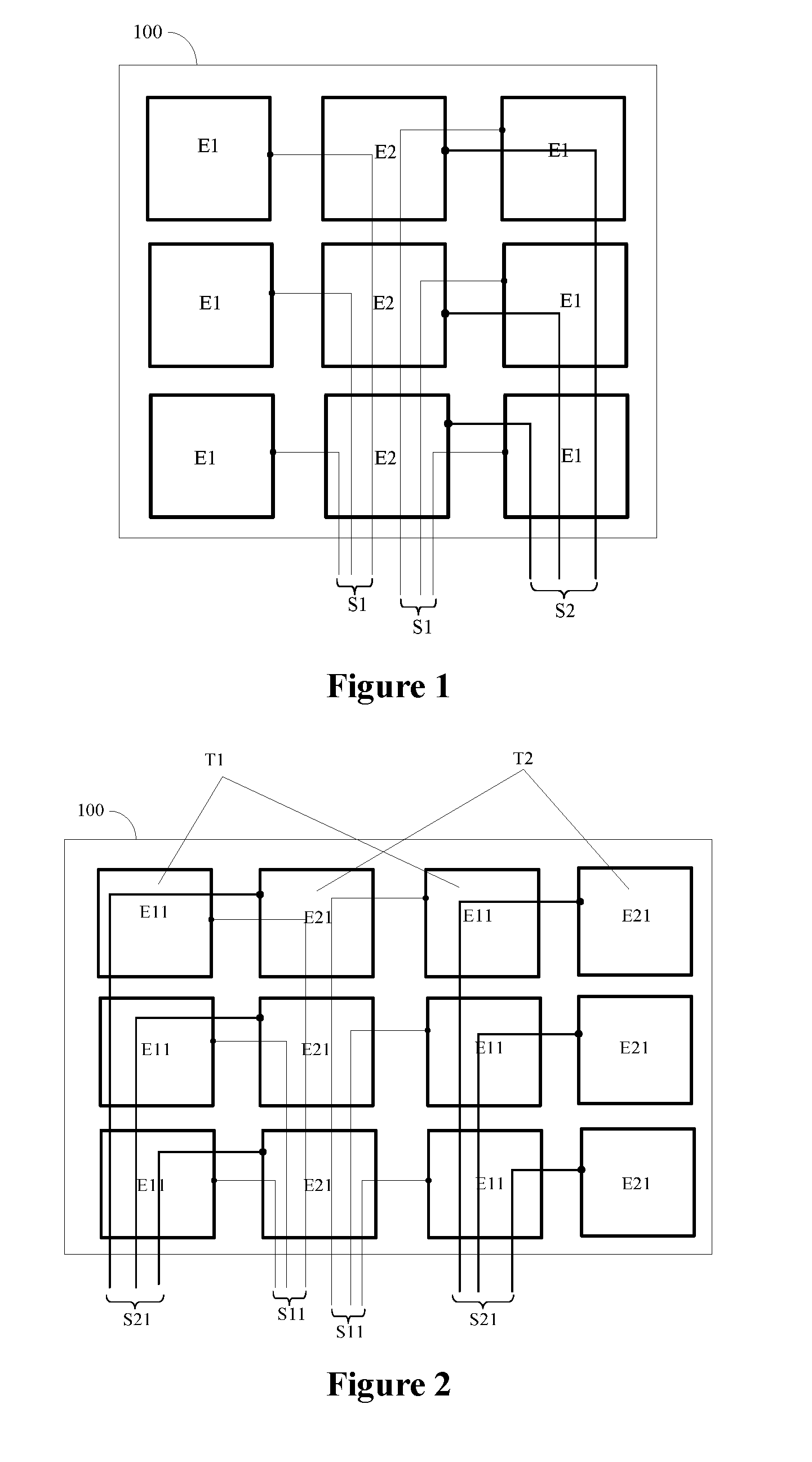
[0042]As is known in the art, wirings of the touch electrode lines in the touch panel are performed in a same direction as far as possible for reducing parasitic capacitance caused by signal wiring to the greatest extent, to acquire minimum parasitic capacitance. In this way the touch electrodes may be grouped, and wirings of touch electrodes in a group may be arranged in the projection regions of touch electrodes in another group in the direction perpendicular to the touch panel, which is described in detail in a

[0043]It should be noted that all touch electrodes are arranged in an array on a substrate, that is, all touch electrodes form a touch electrode array on the substrate. The touch electrode array is arranged to be an N×M array. In the N×M array, there are a first column, a second column . . . to an N-th column of touch electrodes from left to right, and there are a first row, a second row . . . to an M-th row of touch electrodes from top to bottom, where N and M are both int...

third embodiment

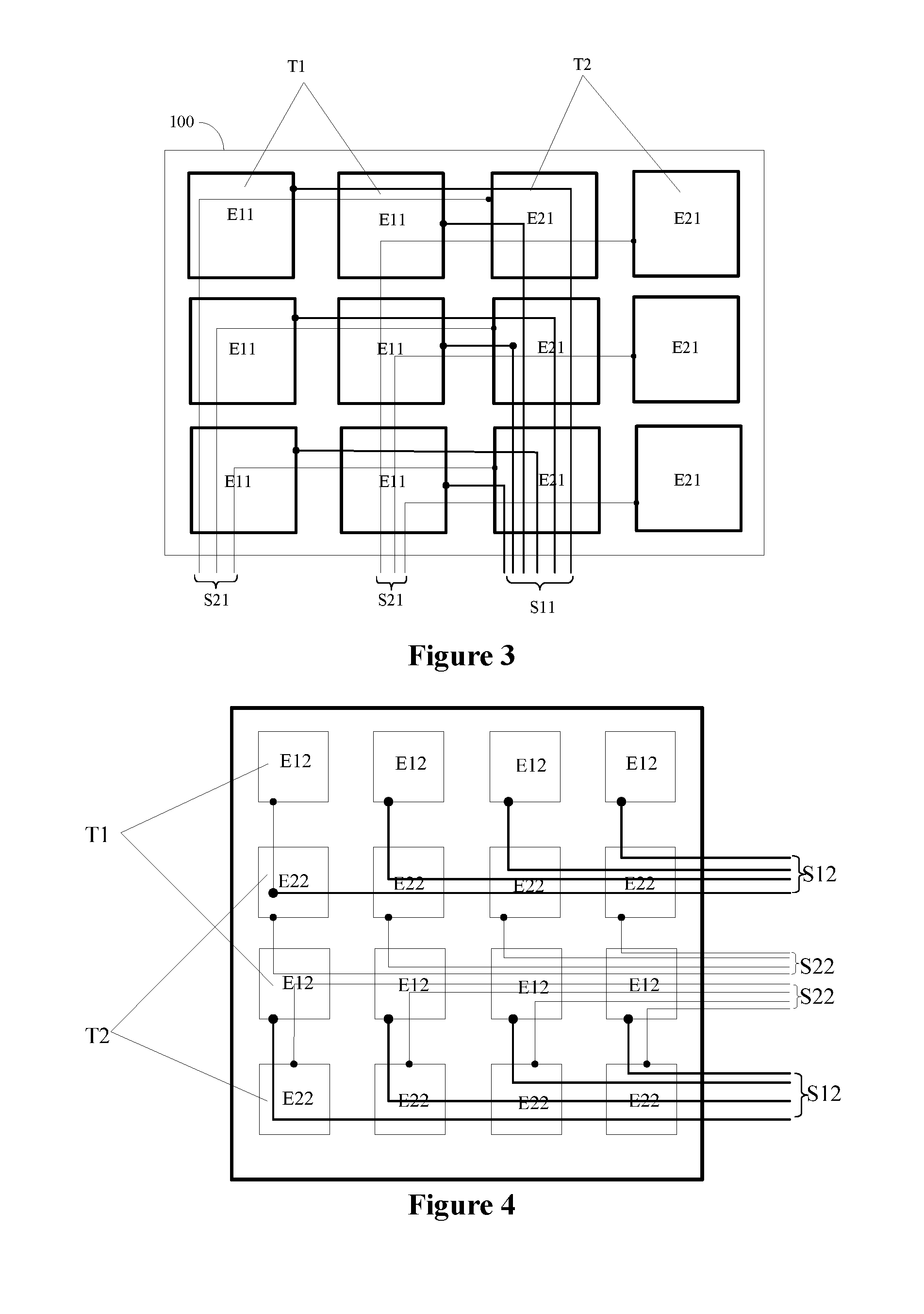
[0061]FIG. 4 is a schematic structural diagram of a touch panel according to the disclosure.

[0062]In the touch panel according to the embodiment of the disclosure, all touch electrodes are arranged in an array on a substrate. The touch electrode array shown in FIG. 4 is a 4×4 array.

[0063]As shown in FIG. 4, the touch electrode array includes a first group T1 of touch electrodes including first touch electrodes and a second group T2 of touch electrodes including second touch electrodes.

[0064]The first group T1 of touch electrodes includes a first row of touch electrodes and a third row of touch electrodes, and the second group T2 of touch electrodes includes a second row of touch electrodes and a fourth row of touch electrodes.

[0065]The touch electrode lines connected to the touch electrodes in the first row are arranged in the projection areas of the touch electrodes in the second row in the direction perpendicular to the touch panel, the touch electrode lines connected to the touch...


PUM


Abstract

A touch panel, a method for driving the touch panel and a touch display device are provided. The touch panel includes a substrate, and multiple touch electrodes and touch electrode lines located on the substrate, the touch electrodes are respectively connected to the touch electrode lines. The touch electrodes include at least a first touch electrode and a second touch electrode, and the touch electrode lines include at least a first touch electrode line and a second touch electrode line. The first touch electrode line is disposed at a position where the first touch electrode line do not overlap with a projection region of other touch electrode driven simultaneously with the first touch electrode in the direction perpendicular to the touch panel.

Description

CROSS REFERENCE TO RELATED APPLICATIONS[0001]The present application claims the priority of Chinese Patent Application No. 201510153141.1, titled “TOUCH PANEL AND METHOD FOR DRIVING THE SAME, AND TOUCH DISPLAY DEVICE”, filed on Apr. 1, 2015 with the State Intellectual Property Office of People's Republic of China, which is incorporated herein by reference in its entirety.FIELD OF THE INVENTION[0002]The disclosure relates to the field of liquid crystal display technologies, and in particular to a touch panel and a method for driving the touch panel, and a touch display device including the touch panel.BACKGROUND OF THE INVENTION[0003]A touch panel includes a substrate and a touch electrode layer located on the substrate, where the touch electrode layer includes multiple touch electrodes insulated from each other and each of the multiple touch electrodes is connected to a respective touch electrode line. When the touch panel is driven, a drive signal is applied to the touch electrode ...

Claims


Application Information

Patent Timeline
Patent Type & Authority Applications(United States)
IPC IPC(8): G06F3/041G06F3/044G06F3/047
CPCG06F3/0416G06F3/047G06F2203/04111G06F3/044G06F3/0412G06F3/04164G06F3/04166G06F3/0443
Inventor ZHAI, YINGTENG
Owner SHANGHAI TIANMA MICRO ELECTRONICS CO LTD
Why Eureka
Try Eureka