Multi-layered circuit board and semiconductor device
a multi-layer circuit board and semiconductor technology, applied in the direction of semiconductor/solid-state device details, cross-talk/noise/interference reduction, printed circuit non-printed electric components association, etc., can solve the problem of degrading the high-frequency characteristics of the multi-layered circuit board
- Summary
- Abstract
- Description
- Claims
- Application Information
AI Technical Summary
Benefits of technology
Problems solved by technology
Method used
Image
Examples
first embodiment
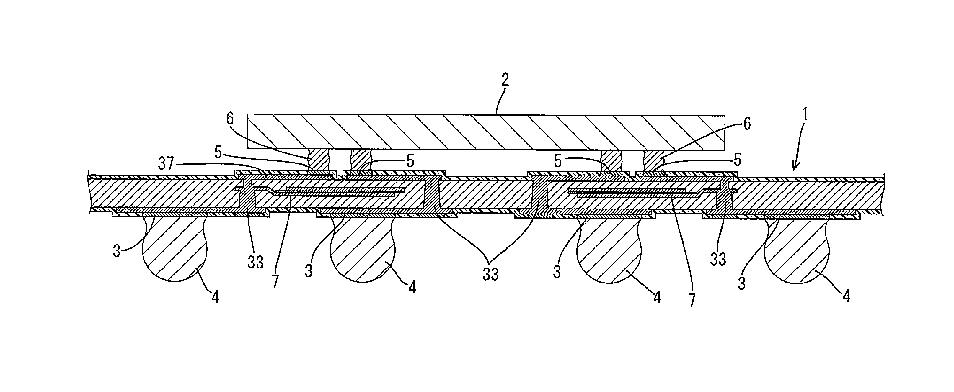
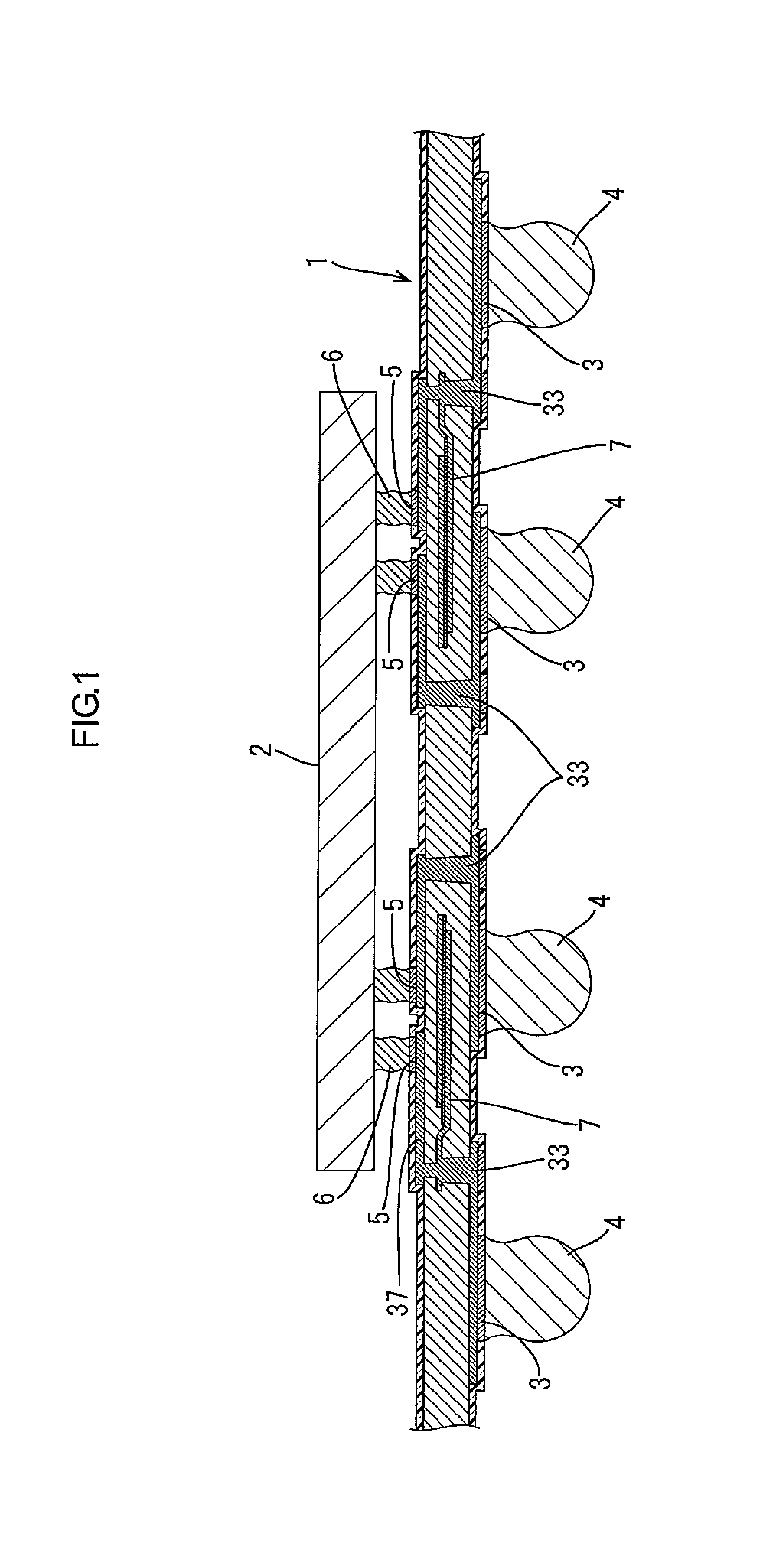
[0045]A first embodiment of the present invention will be described with reference to FIGS. 1 to 18.
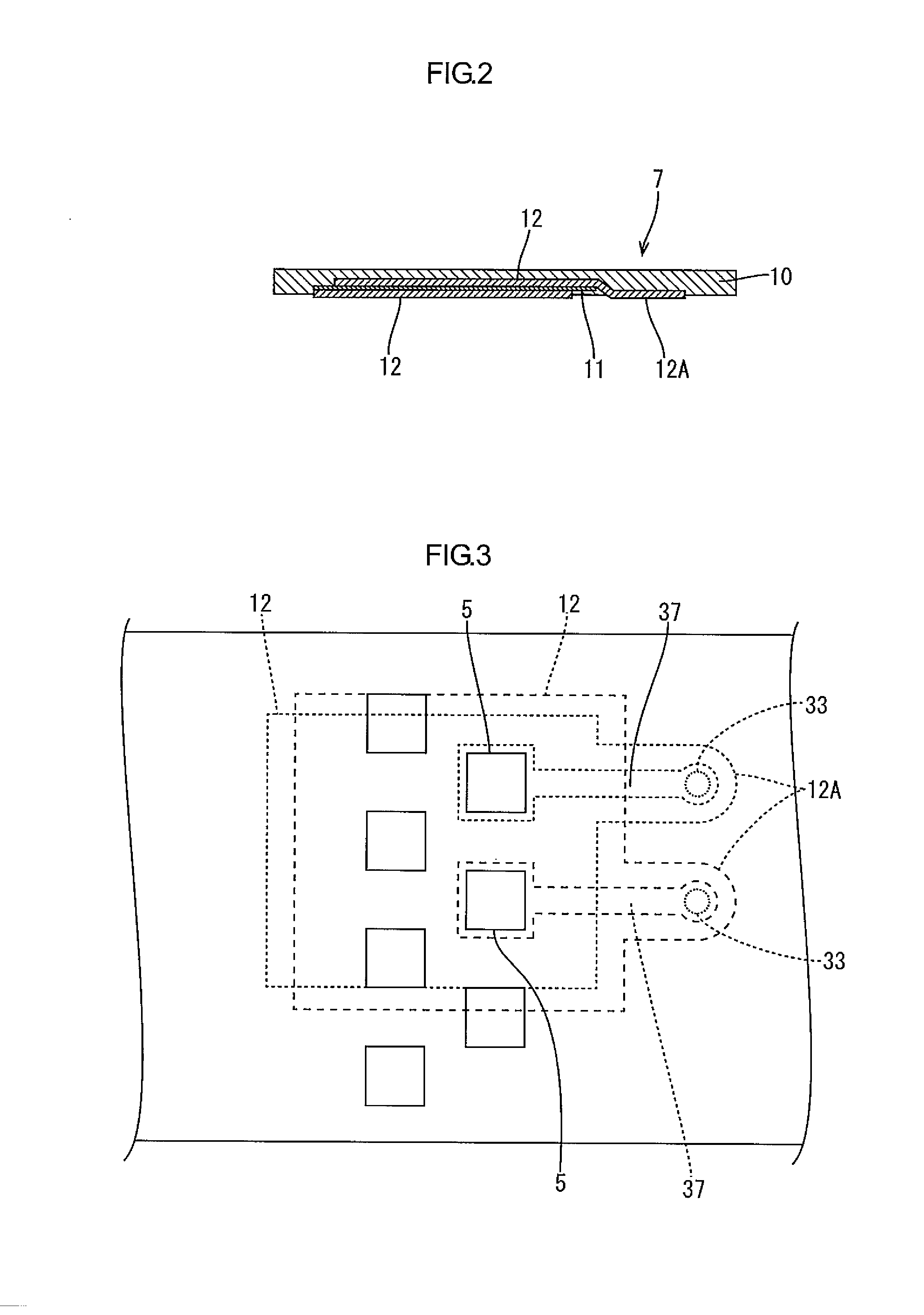
[0046]A package including an LSI 2 and a multi-layered circuit board 1 that is used as a relay board according to the first embodiment is illustrated in FIG. 1. External connection pads 3 are formed on a lower surface of the multi-layered circuit board 1. Solder balls 4 for external connection are formed on the external connection pads 3. Chip connecting pads 5 are formed on an upper surface of the multi-layered circuit board 1 at positions corresponding to pads of the LSI 2, which are not illustrated. The multi-layered circuit board 1 is connected to the LSI 2 with micro solder balls 6 formed on the chip connecting pads 5. The multi-layered circuit board 1 includes sheet capacitors 7 therein. The sheet capacitors 7 are located between multiple pairs of power supply terminals and ground terminals of the LSI 2. The sheet capacitors 7 function as bypass capacitors. The chip connecting p...
second embodiment
[0075]A second embodiment of the present invention will be described with reference to FIG. 19. In the following description, components and portions having the same configuration to those of the first embodiment will be indicated by the same numerals and will not be described for simplification of illustration.
[0076]As illustrated in FIG. 19, a multi-layered circuit board 41 according to this embodiment includes plate electrodes 12 with tabs 12A at opposite edges included in the sheet capacitors 7. The interlayer connecting conductors 33 and the lead wiring 37 are formed on the tabs 12A, respectively, and connected to the corresponding chip connecting pad 5.
[0077]Each lead wiring 37 connected to each tab 12 is arranged so as to overlap the plate electrodes 12 of the sheet capacitors 7, when viewed from the stacking direction of the multi-layered circuit board 41. The chip connecting pad 5 is formed on common portion of the lead wirings 37 connected to the corresponding plate electr...
third embodiment
[0081]A third embodiment of the present invention will be described with reference to FIGS. 20 to 23. In the following description, components and portions having the same configuration to those of the first embodiment will be indicated by the same numerals and will not be described for simplification of illustration. A difference between the first embodiment and the third embodiment is a configuration for forming each current path in which a current flows back and forth, that is, a configuration of each return-type capacitor.
[0082]As illustrated in FIG. 20, an LSI package (an example of a semiconductor device) 100 includes a multi-layered circuit board (an example of a circuit board) 1 and an LSI (an example of a semiconductor chip) 2. The LSI package 100 includes the return-type capacitors different from the return-type capacitors in the LSI package of the first embodiment illustrated in FIG. 1. Other configurations of the LSI package 100 are the same as those of the LSI package o...
PUM
 Abstract
Description
Claims
Application Information
 - R&D
- Intellectual Property
- Life Sciences
- Materials
- Tech Scout
- Unparalleled Data Quality
- Higher Quality Content
- 60% Fewer Hallucinations
Browse by: Latest US Patents, China's latest patents, Technical Efficacy Thesaurus, Application Domain, Technology Topic, Popular Technical Reports.
© 2025 PatSnap. All rights reserved.Legal|Privacy policy|Modern Slavery Act Transparency Statement|Sitemap|About US| Contact US: help@patsnap.com


