
Solar cell having three-dimensional p-n junction structure and method for manufacturing same

Active Publication Date: 2016-08-18
DAEGU GYEONGBUK INST OF SCI & TECH
View PDF8 Cites 2 Cited by
  • Summary
  • Abstract
  • Description
  • Claims
  • Application Information

AI Technical Summary

Benefits of technology

This patent describes a new method for making a 3-dimensional P-N junction solar cell. The method involves coating a base board with a back plate, and then sequentially adding layers of a P type semiconductor material, a N type buffer layer, and a transparent electrode. The resulting solar cell has a 3-dimensional structure with a high surface-to-volume ratio, which makes it more efficient than traditional solar cells. Additionally, this patent also describes a method for preparing a porous CZTS thin film, which can be used as a light absorption layer in solar cells. The technical effects of this patent include improved efficiency and better light absorption in solar cells.

Problems solved by technology

The said silicon solar cell has the advantage of high photo conversion efficiency but has the disadvantage of high production costs.
However, since the highly expensive raw materials such as In and Ga are necessary for the production of CIS or CIGS thin film solar cell, the effort to lower the manufacturing costs with the raw materials is limited.
This method has the advantage of easiness in controlling the chemical composition, phase behavior of the thin film, microstructure of the thin film, and reproducibility, but has the disadvantage of high costs.
To perform the non-vacuum process, an organic binder is necessary to secure the coating property, and the resulting carbon residue is a problem.
The morphology of the thin film is also limited in this method.

Method used

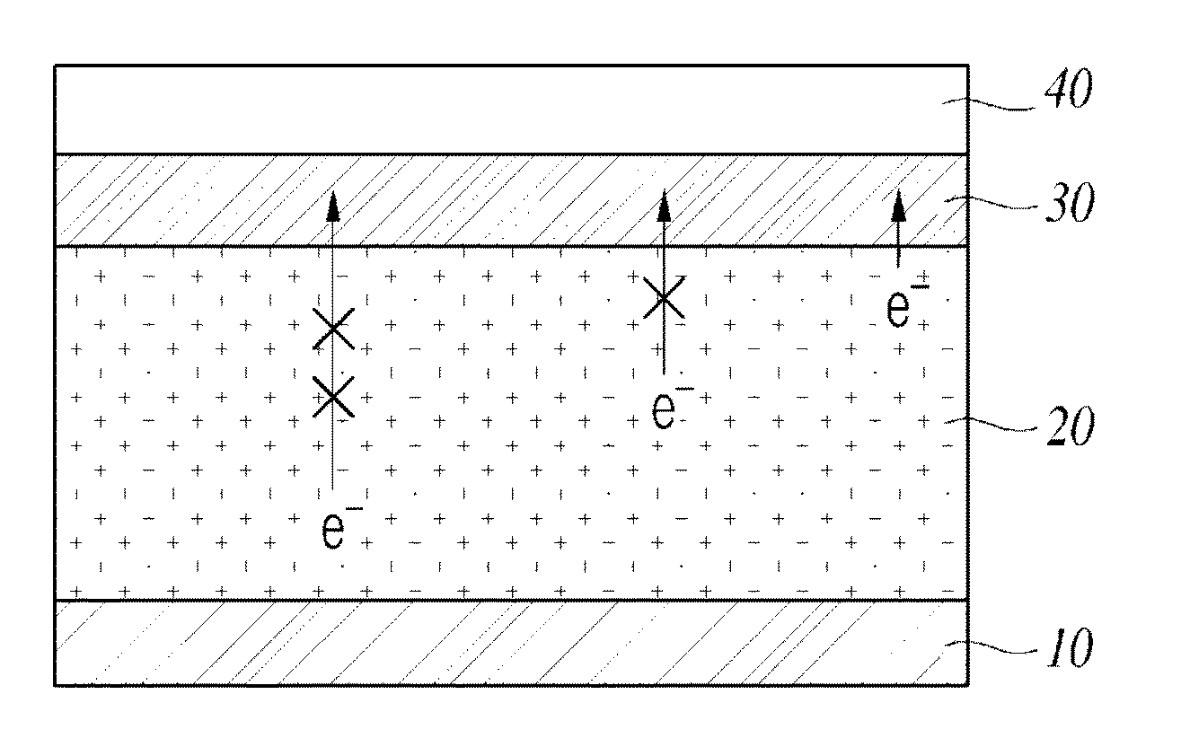
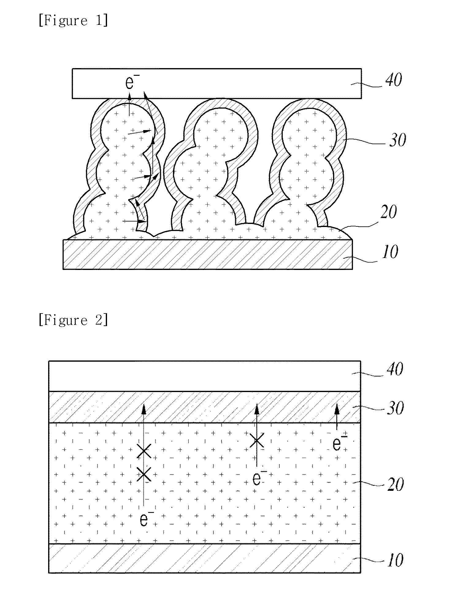
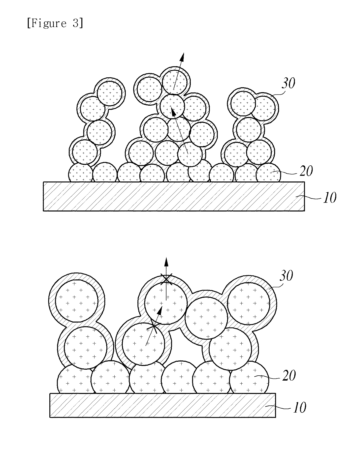

Image

  • Solar cell having three-dimensional p-n junction structure and method for manufacturing same
  • Solar cell having three-dimensional p-n junction structure and method for manufacturing same
  • Solar cell having three-dimensional p-n junction structure and method for manufacturing same

Examples


manufacturing example 1

[0138]A porous CZTS thin film was prepared by the following steps.

[0139]Step 1: A CZTS precursor solution was prepared by mixing the copper precursor (CuCl2, 0.9 M), zinc precursor (ZnCl2, 0.7 M), tin precursor (SnCl2, 0.5 M), and sulfur precursor (CH4N2S (thiourea), 4 M) with the mixed solvent composed of ultrapure water and ethanol at the ratio of 7:3.

[0140]Step 2: The base board (ex: glass, metal foil, plastic board, etc.) having Mo electrode formed thereon was coated with the precursor solution above via spin coating.

[0141]Step 3: The coated thin film was pre-heated at 350° C.

[0142]Step 4: The pre-heated thin film was heated at 500° C. for 20 minutes in sulfur atmosphere.

manufacturing example 2

[0143]A porous CZTS thin film was prepared by the same manner as described in Manufacturing Example 1 except that the sulfurization in step 4 was performed at 530° C.

manufacturing example 3

[0144]A porous CZTS thin film was prepared by the same manner as described in Manufacturing Example 1 except that the sulfurization in step 4 was performed at 550° C.


PUM


Abstract

The present invention provides a 3-dimensional P-N junction solar cell composed of a base board coated with a back plate on the upper face of the same; a P type semiconductor thin film formed on the top side of the back plate which has a 3-dimensional porous structure and is composed of P type semiconductor crystal grains; a N type buffer layer formed on the surface of the crystal grains of the said P type semiconductor thin film with playing a role of coating the thin film; and a transparent electrode formed on the surface of the crystal grains of the P type semiconductor thin film on which the N type buffer layer is formed. The solar cell of the present invention is a P-N junction solar cell including a 3-dimensional photo catalytic thin film, which can provide an improved photoelectric conversion efficiency, compared with the conventional P-N junction solar cell, owing to the formation of the N-type buffer layer on the surface of the crystal grains of the 3-dimensional P type semiconductor thin film.

Description

BACKGROUND OF THE INVENTION[0001]1. Field of the Invention[0002]The present invention relates to a 3-dimensional P-N junction solar cell and the preparation method of the same.[0003]2. Description of the Related Art[0004]The solar cell that can generate electricity directly from the sunlight is the most promising future energy production method, considering it is advantageous for producing a clear energy safely. To construct such a solar cell, a variety of inorganic and organic semiconductors have been applied. However, the most representative products succeeded in the commercialization so far are the silicon solar cell comprising silicon (Si) as a major material and the CIGS thin film solar cell.[0005]The said silicon solar cell has the advantage of high photo conversion efficiency but has the disadvantage of high production costs. As an alternative, a thin film solar cell is attracting our interests which uses a compound semiconductor where a thinner layer can be applied. The repr...

Claims


Application Information

Patent Timeline
IPC IPC(8): H01L31/0352H01L31/0224H01L31/18H01L31/072H01L31/0749H01L31/032H01L31/0445
CPCH01L31/072H01L31/0326H01L31/035281H01L31/0445H01L31/18H01L31/022466H01L31/0322H01L31/0749Y02E10/50H01L31/0352Y02E10/541
Inventor SUNG, SHI-JOONPARK, SI-NAEKIM, DAE-HWANKANG, JIN-KYUHWANG, DAE-KUE
Owner DAEGU GYEONGBUK INST OF SCI & TECH
Learn More