
Methods of forming nanoscale conductive films and touch devices including the nanoscale conductive films

a nano-scale conductive film and nano-scale technology, applied in the field of conductive films, can solve the problems of insufficient etching, large haze change after etching, uneven etching, etc., and achieve the effects of reducing manufacturing time, reducing damage on overcoats, and maintaining the optical characteristics of nano-scale conductive films

Active Publication Date: 2016-05-12
TRENDON TOUCH TECHNOLOGY CORPORATION
View PDF3 Cites 4 Cited by
  • Summary
  • Abstract
  • Description
  • Claims
  • Application Information

AI Technical Summary

Benefits of technology

The methods described in this patent can effectively create nanoscale conductive films with electrical isolation and minimal damage to the overcoat. Additionally, the methods require less manufacturing time and lead to no visible difference in optical performance between conductive and non-conductive regions. These features make the films more suitable for use in touch-panel display devices, improving their appearance.

Problems solved by technology

However, it has always been an important topic in the touch panel industry to seek an alternative material for ITO conductive films, no matter whether the motivation is due to the fact that ITO has disadvantages (such as brittleness and inflexibility) or for cost reduction.
Nevertheless, the overcoat may on the other hand significantly reduce the interaction between the etchant and the SNW, resulting in uneven etch, insufficient etch and a large haze change after etch.
Moreover, residue of the etchant may be left over after the etching process, which may cause a subsequently formed SNW conductive film to degrade in electrical characteristics.
However, such etching processes may not effectively protect the overcoat and thus the SNW conductive film may be liable to degrade in electrical characteristics.

Method used


Image

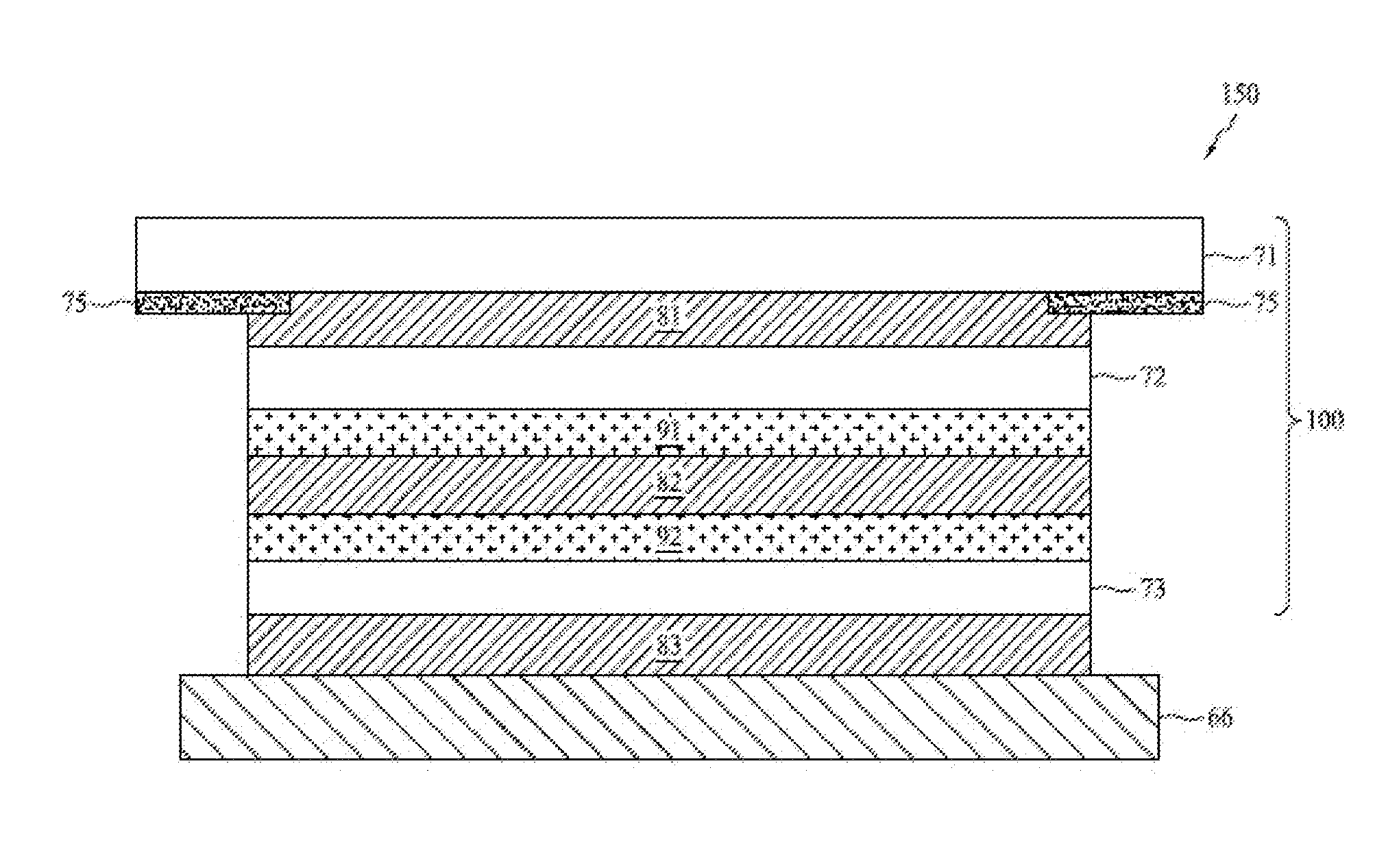
  • Methods of forming nanoscale conductive films and touch devices including the nanoscale conductive films
  • Methods of forming nanoscale conductive films and touch devices including the nanoscale conductive films
  • Methods of forming nanoscale conductive films and touch devices including the nanoscale conductive films

Examples


Embodiment Construction

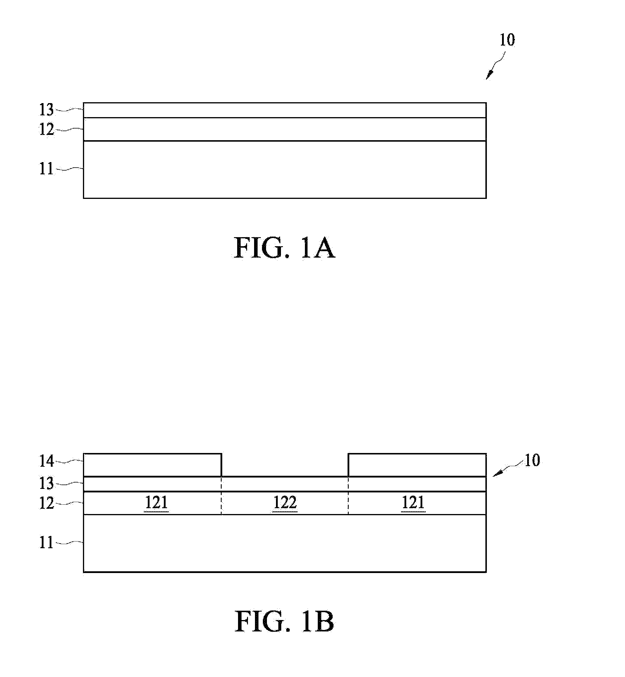
[0057]The embodiments of the disclosure are shown in the following description with the drawings, wherein similar or same components are indicated by similar reference numbers.

[0058]FIGS. 1A to 1D are schematic diagrams showing a method of manufacturing a nanoscale conductive film, in accordance with various embodiments of the disclosure. Referring to FIG. 1A, initially a nano base film 10 is provided, according to the method. The nanoscale base film 10 includes a substrate 11, a first overcoat 13 on one side of the substrate 11, and a first nano material layer 12 laminated between the substrate 11 and the first overcoat 13. In some embodiments, the substrate 11 includes a flexible, optically transmissive material such as polyethylene terephthalate (PET). In addition, the first overcoat 13 includes a material that is organic and porous. Moreover, the first nano material layer 12 includes silver nanowire (SNW) in a wire grid pattern having a reduced wire diameter below 100 nanometers...


PUM

PropertyMeasurementUnit
hazeaaaaaaaaaa
hazeaaaaaaaaaa
diameteraaaaaaaaaa

Abstract

The present disclosure provides a method of forming a nanoscale conductive film. The method comprises providing a nanoscale base film, forming a first patterned insulating layer on the nanoscale base film, and etching the nanoscale base film in a current generation system, using the first patterned insulating layer as a mask. The nanoscale base film includes a substrate, a first overcoat on one side of the substrate, and a first nano material layer laminated between the substrate and the first overcoat. The first patterned insulating layer is formed on the first overcoat, exposing portions of the first overcoat. In the first nano material layer, first regions are masked by the first insulating layer and second regions are not masked by the first insulating layer. The first regions and the second regions are electrically isolated from each other after etching the nanoscale base film in the current generation system.

Description

BACKGROUND OF THE INVENTION[0001]This application claims priority to China Application Serial Number 201410624691.2, filed Nov. 7, 2014, which is herein incorporated by reference.[0002]1. Filed of the Invention[0003]The present disclosure relates to conductive films and, more particularly, to a method of forming a nanoscale conductive film and a touch device including the nanoscale conductive film.[0004]2. Related Art of the Invention[0005]Touch panels or touch screens have become more and more popular in electronic devices including, in particular, portable or hand-held devices such as personal digital assistants (PDAs) and mobile phones. In some touch-panel display devices, indium tin oxide (ITO) is still a required transparent conductive material. However, it has always been an important topic in the touch panel industry to seek an alternative material for ITO conductive films, no matter whether the motivation is due to the fact that ITO has disadvantages (such as brittleness and...

Claims


Application Information

Patent Timeline
Patent Type & Authority Applications(United States)
IPC IPC(8): G06F3/041H01B13/34
CPCG06F3/0412H01B13/34B82Y15/00B82Y40/00G06F2203/04103C23F4/00G06F3/041H01L21/3065H01L21/321
Inventor YANG, SHUN-JIESHAO, HONG-SIANGCHANG, EN-CHINLIN, HIS-CHIEN
Owner TRENDON TOUCH TECHNOLOGY CORPORATION
Learn More