Thin film transistor element, production method for same, and display device
- Summary
- Abstract
- Description
- Claims
- Application Information
AI Technical Summary
Benefits of technology
Problems solved by technology
Method used
Image

Examples
embodiment 1
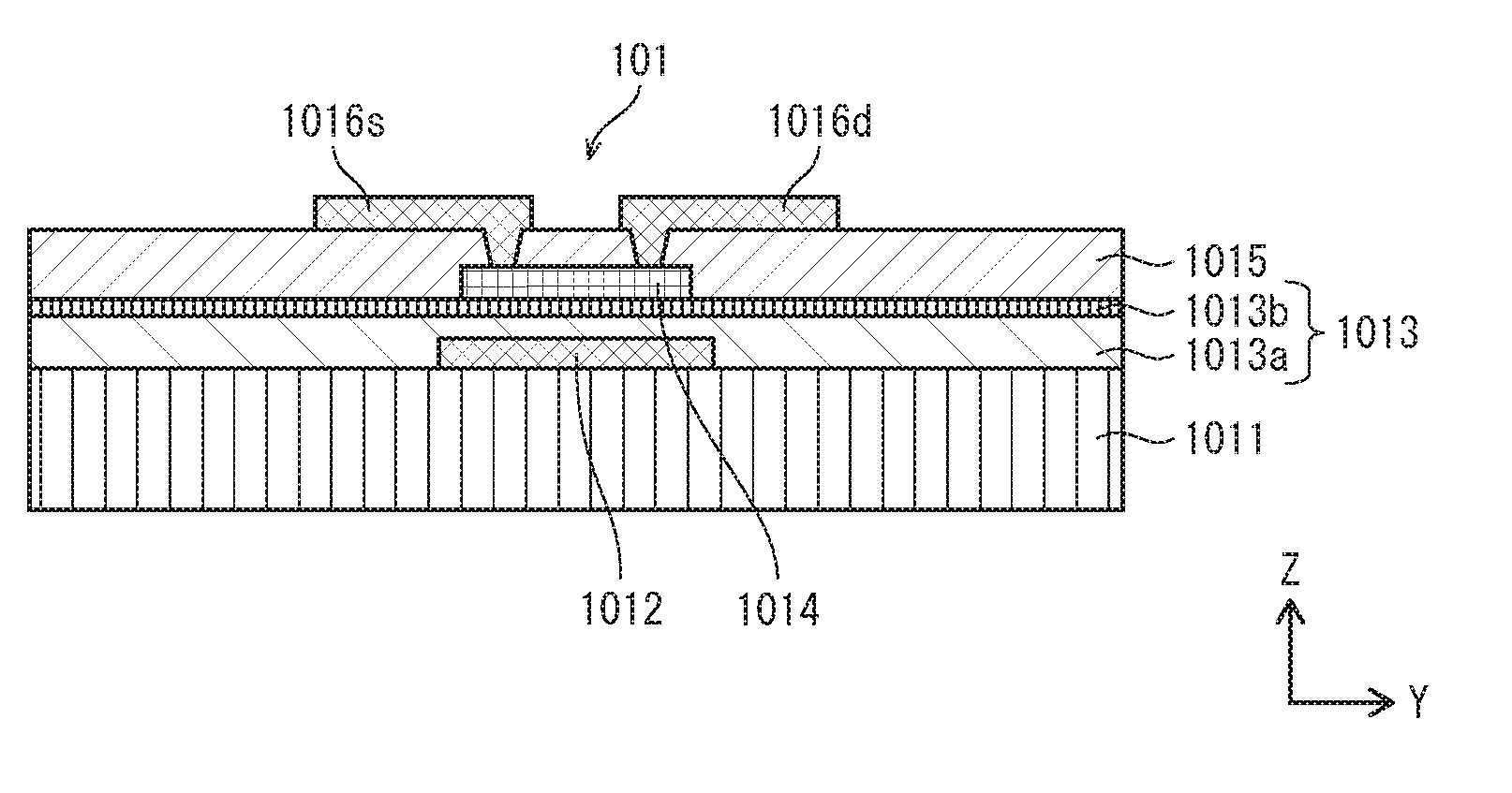
[0045]The following explains, as one aspect of the present disclosure, a TFT 101 relating to Embodiment 1 that is a bottom gate TFT with a channel protection layer.
[0046]1. Cross-Sectional Structure of TFT 101
[0047]A cross-sectional structure of the TFT 101 is explained with reference to FIG. 1.
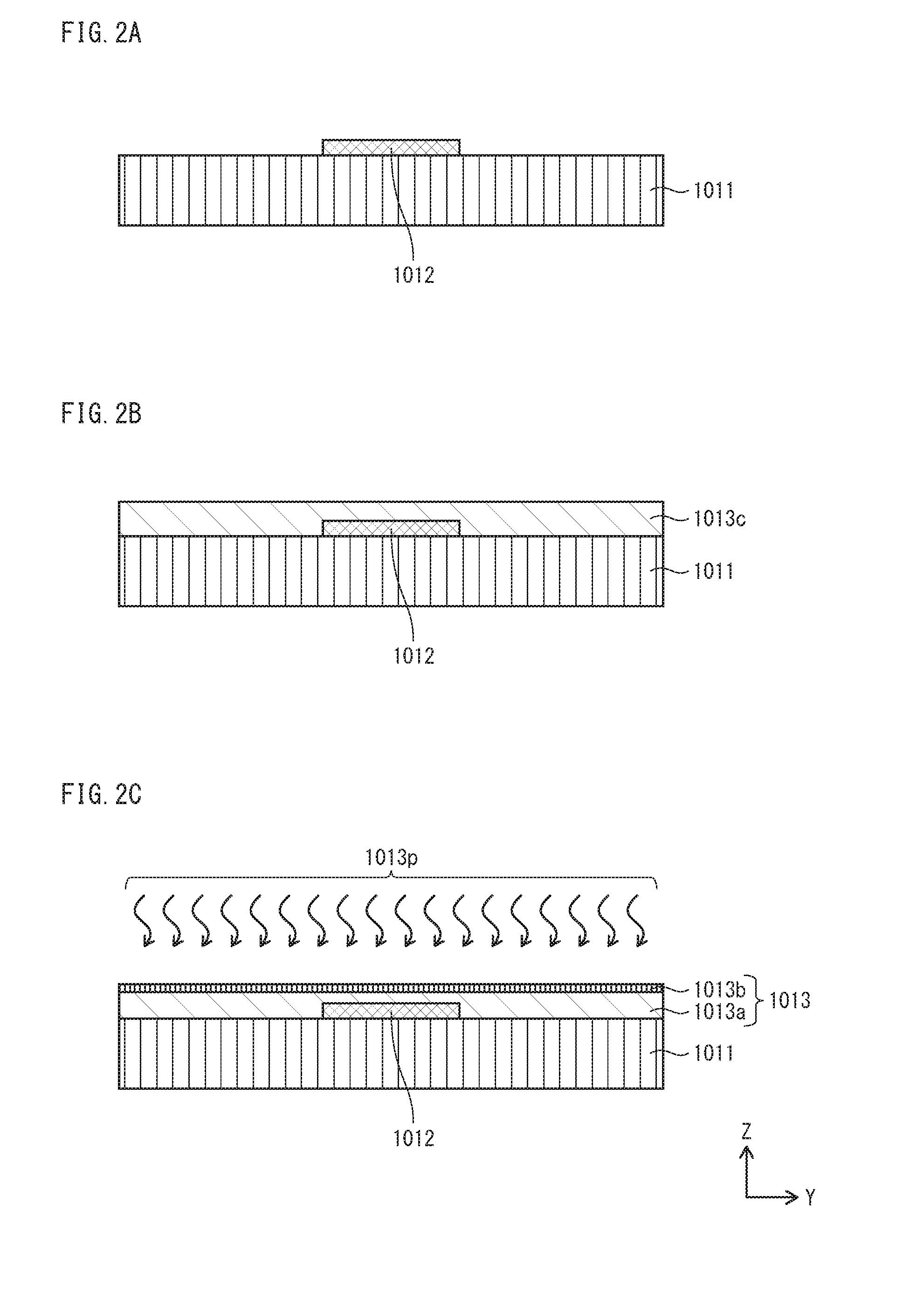
[0048]As shown in FIG. 1, in the TFT 101, a gate electrode 1012 is formed on a substrate 1011, and a gate insulating layer 1013 is formed on the substrate 1011 so as to cover the gate electrode 1012.
[0049]Here, the gate insulating layer 1013 includes a first gate insulating layer 1013a and a second gate insulating layer 1013b. The first gate insulating layer 1013a is formed on the substrate 1011 so as to cover the gate electrode 1012, as a layer that is positioned lower in a Z-axis direction (positioned on the side of a lower surface) of the gate insulating layer 1013. The second gate insulating layer 1013b is formed on the first gate insulating layer 1013a, as a layer that is positioned uppe...
embodiment 2
[0145]The following explains, as one aspect of the present disclosure, a TFT 301 relating to Embodiment 2 that is a bottom gate TFT with a channel etching structure, with reference to FIGS. 7A-7C and 8A-8C. FIGS. 7A-7C and 8A-8C correspond to FIGS. 2A-2C and 3A-3C, respectively.
[0146]1. Cross-Sectional Structure of TFT 301
[0147]FIG. 8C is a schematic cross-sectional view showing the TFT 301. As shown in FIG. 8C, a substrate 3011, a gate electrode 3012, a gate insulating layer 3013 including a first gate insulating layer 3013a and a second gate insulating layer 3013b, a channel layer 3014 have the same structures as those included in the TFT 101 relating to Embodiment 1 shown in FIG. 1.
[0148]As shown in FIG. 8C, on the other hand, the TFT 301 does not include the channel protection layer 1015, which is included in the TFT 101. Also, a source electrode 3016s and a drain electrode 3016d are directly formed with an interval therebetween on the gate insulating layer 3013 and the channel ...
embodiment 3
[0162]The following explains, as one aspect of the present disclosure, a TFT 401 relating to Embodiment 3 that is a top gate TFT, with reference to FIGS. 9A-9D and 10A-10C. FIGS. 9A-9D and 10A-10C correspond to FIGS. 2A-2C and 3A-3C, respectively.
[0163]1. Cross-Sectional Structure of TFT 401
[0164]FIG. 10C is a schematic cross-sectional view showing the TFT 401. As shown in FIG. 10C, in the TFT 401, a channel layer 4014 is formed on a substrate 4011, and a gate insulating layer 4013 is formed on the substrate 4011 so as to cover the channel layer 4014. The gate insulating layer 4013 includes a second gate insulating layer 4013b in a region thereof that is in contact with the substrate 4011 and the channel layer 4014, and includes a first gate insulating layer 4013a on an upper surface of the second gate insulating layer 4013b.
[0165]Also, a gate electrode 4012 is formed on the gate insulating layer 4013, and an interlayer insulating layer 4015 is formed on the gate insulating layer 4...
PUM
 Abstract
Description
Claims
Application Information
 - R&D
- Intellectual Property
- Life Sciences
- Materials
- Tech Scout
- Unparalleled Data Quality
- Higher Quality Content
- 60% Fewer Hallucinations
Browse by: Latest US Patents, China's latest patents, Technical Efficacy Thesaurus, Application Domain, Technology Topic, Popular Technical Reports.
© 2025 PatSnap. All rights reserved.Legal|Privacy policy|Modern Slavery Act Transparency Statement|Sitemap|About US| Contact US: help@patsnap.com