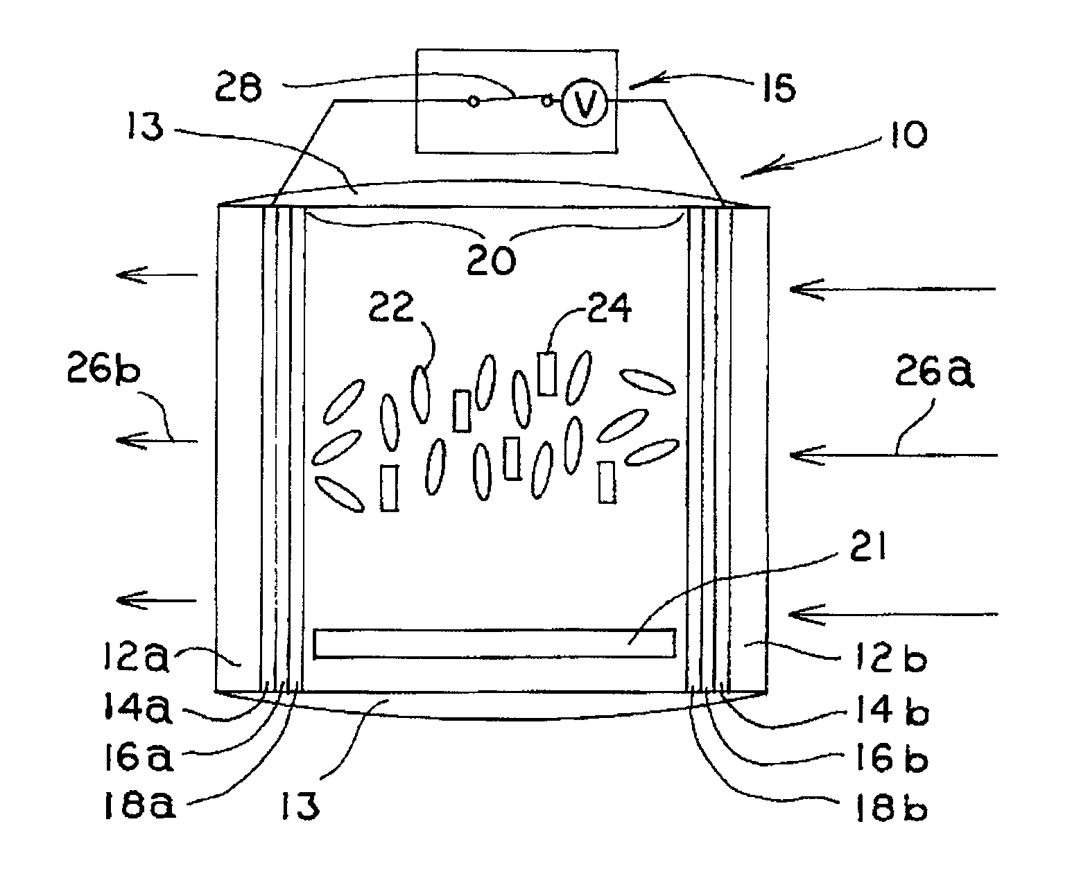
Wide band variable transmittance optical device
a transmittance optical and wide band technology, applied in the field of wide band variable transmittance optical devices, can solve the problems of limiting the amount of light transmission of the device, no current commercial liquid crystal guest-host device that provides wideband absorption greater than 175 nm for eyewear applications, and inacceptable eyewear applications, etc., to achieve the effect of reducing the transmission of ligh
- Summary
- Abstract
- Description
- Claims
- Application Information
AI Technical Summary
Benefits of technology
Problems solved by technology
Method used
Image
Examples
example 1
[0120]A variable transmission cell was prepared according to the following protocol. A test cell was fabricated using substrates of 5 mil polyethylene terephthalate (PET) pre-coated with a conducting polymer (Kimoto Tech, Cedartown Ga., U.S.A.). The conductive polymer served as a transparent electrode. On top of the conducting polymer, a coating of polyimide, Nissan SE1211 (Nissan Chemical Industries, Ltd., Tokyo, Japan), was applied by silk-screening and then baked at 100° C. for 2 hours. This polyimide coating served as an alignment layer designed to induce a substantially homeotropic surface alignment of the liquid crystal molecules. Next, Shinshikyu EW plastic spheres, 6 micron in diameter, (Hiko Industrial Ltd, Hong Kong) were sprayed onto one of the substrates to act as spacers. A thin bead of UV curable adhesive, Loctite 3106, (Henkel AG & Co. KGaA, Dusseldorf, Germany) was then applied around the perimeter of one of the substrates, leaving a gap that would serve as a fill po...
example 2
[0123]A variable transmission cell was prepared according to the following protocol. A test cell was fabricated using substrates of 3 mil polyethylene terephthalate (PET) pre-coated with a transparent conducting ITO (Techimat, U.S.A.). On top of the conducting polymer, a coating of polyimide, Nissan SE1211 (Nissan Chemical Industries, Ltd., Tokyo, Japan), was applied by silk-screening and then baked at 100° C. for 2 hours. This polyimide coating served as an alignment layer designed to induce a substantially homeotropic surface alignment of the liquid crystal molecules. Next, Shinshikyu EW plastic spheres, 6 micron in diameter, (Hiko Industrial Ltd, Hong Kong) were sprayed onto one of the substrates to act as spacers. A thin bead of UV curable adhesive, Loctite 3106, (Henkel AG & Co. KGaA, Dusseldorf, Germany) was then applied around the perimeter of one of the substrates, leaving a gap that would serve as a fill port. The two substrates were then assembled, pressed together against...
example 3
[0126]A variable transmission cell having a positive mixture was prepared according to the following protocol. A test cell was fabricated using substrates of 3 mil polyethylene terephthalate (PET) coated with Indium Thin Oxide (ITO), a transparent conductor. On top of the ITO, a coating of polyimide, Nissan 5291 (Nissan Chemical Industries, Ltd., Tokyo, Japan), was spin coated. This polyimide coating served as an alignment layer designed to induce a strong planar alignment of the liquid crystal molecules. Next, L-34N black plastic spheres, 9.4 microns in diameter, (Hayakawa Rubber Co., Ltd, Hiroshima Japan) were sprayed onto one of the substrates to act as spacers. A thin bead of UV-curable adhesive, Loctite 3106, (Henkel AG & Co. KGaA, Dusseldorf, Germany) was then applied around the perimeter of one of the substrates, leaving a gap that would serve as a fill port. The two substrates were then assembled, pressed together against the spacers to create a uniform gap between the subst...
PUM
 Abstract
Description
Claims
Application Information
 - R&D
- Intellectual Property
- Life Sciences
- Materials
- Tech Scout
- Unparalleled Data Quality
- Higher Quality Content
- 60% Fewer Hallucinations
Browse by: Latest US Patents, China's latest patents, Technical Efficacy Thesaurus, Application Domain, Technology Topic, Popular Technical Reports.
© 2025 PatSnap. All rights reserved.Legal|Privacy policy|Modern Slavery Act Transparency Statement|Sitemap|About US| Contact US: help@patsnap.com


