Thermochemical gas sensor using chalcogenide-based nanowires and method for manufacturing the same
a technology of chalcogenide-based nanowires and gas sensors, which is applied in the manufacture/treatment of thermoelectric devices, instruments, and the construction details of gas analysers, etc., can solve the problems of difficulty in manufacturing a low-priced sensor, and achieve the effect of maximum thermoelectric properties, specific surface area, and characteristic electrical and optical properties
- Summary
- Abstract
- Description
- Claims
- Application Information
AI Technical Summary
Benefits of technology
Problems solved by technology
Method used
Image
Examples
example 1
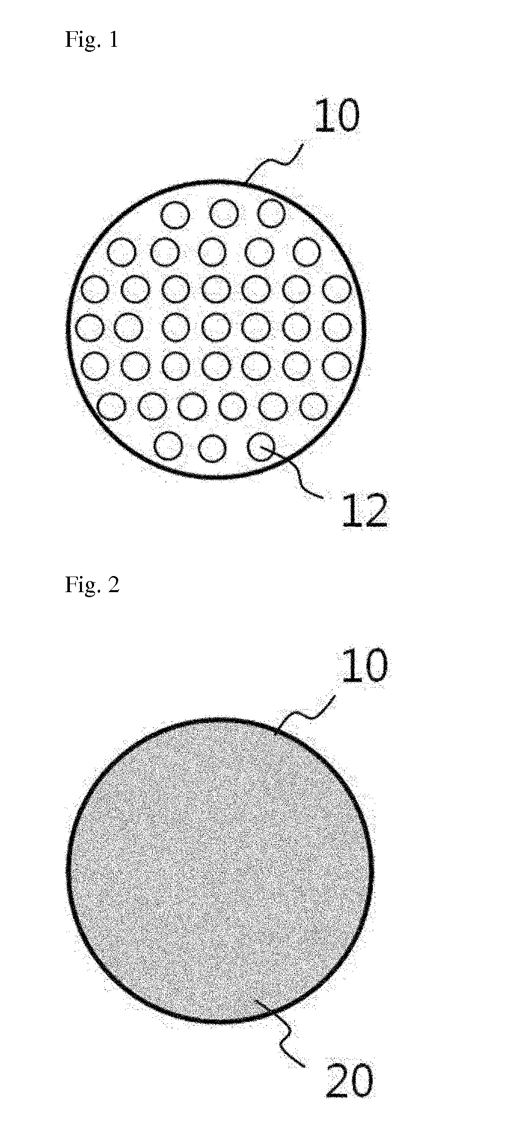
[0111]To manufacture a thermochemical gas sensor in this example, a porous alumina template having a diameter of 12 mm and a pore diameter of 200 nm was used as a matrix of the sensor, and electrodeposition was used to form chalcogenide-based nanowires in the porous alumina template.
[0112]To form a single thermoelectric device in the porous alumina template, a sputtering process was performed on a bottom surface of the alumina template, thereby forming a gold seed layer. The height of the gold seed layer formed as described above was detected at approximately 200 nm.
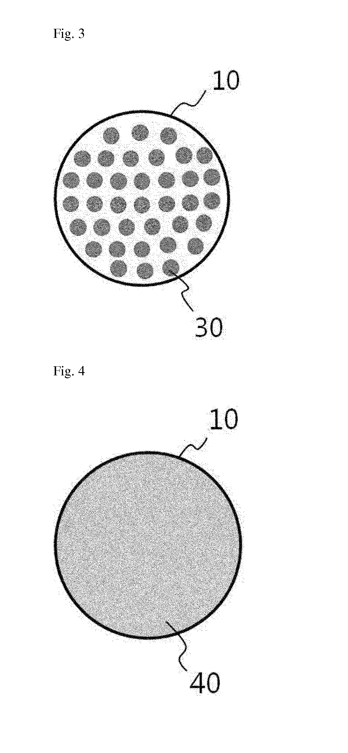
[0113]The gold seed layer exposed through pores formed in the top surface of the porous alumina template was grown by electroplating for 8 hours with a voltage of 75 mV in a three-electrode system using a predetermined rectifier to form BixTey (1.5≦x≦2.5, 2.4≦y≦3.6) nanowires. Here, as an electrolyte, a mixture of 1 M of HNO3, 70 mM of Bi(NO3)3 5H2O and 10 mM of TeO2 was used.
[0114]An electrode in contact with the BixTey...
example 2
[0121]A porous alumina template having a diameter of 12 mm and a pore diameter of 200 nm was used as a matrix of the sensor to manufacture a thermochemical gas sensor in this example, and electrodeposition was used to form chalcogenide-based nanowires in the porous alumina template.
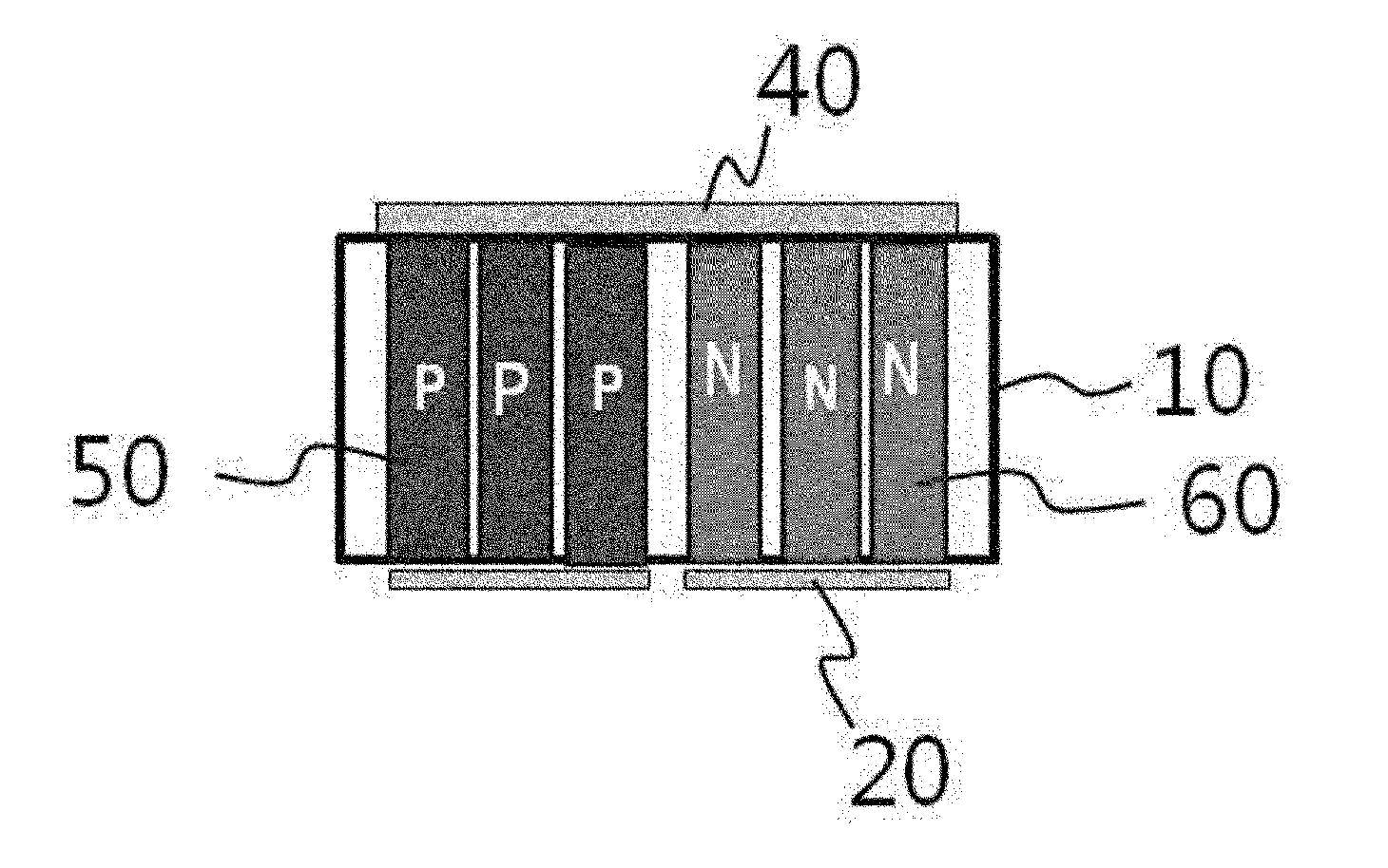
[0122]A process of forming a P-N junction thermoelectric device in the porous alumina template was performed.
[0123]First, masking was performed using stencil, except the part in which the nanowires were to be plated, and a sputtering process was performed on the exposed part, thereby forming a gold seed layer. The height of the gold seed layer formed as such was detected at approximately 200 nm.
[0124]Afterward, to synthesize P-type SbxTey (1.5≦x≦2.5, 2.4≦y≦3.6) nanowires, the part in which N-type BixTey (1.5≦x≦2.5, 2.4≦y≦3.6) nanowires were to be synthesized was masked using a microstop, and the SbxTey nanowires were grown and formed on the gold seed layer exposed through pores on the top surface of the p...
PUM
| Property | Measurement | Unit |
|---|---|---|
| diameter | aaaaa | aaaaa |
| diameter | aaaaa | aaaaa |
| thickness | aaaaa | aaaaa |
Abstract
Description
Claims
Application Information
 - R&D
- Intellectual Property
- Life Sciences
- Materials
- Tech Scout
- Unparalleled Data Quality
- Higher Quality Content
- 60% Fewer Hallucinations
Browse by: Latest US Patents, China's latest patents, Technical Efficacy Thesaurus, Application Domain, Technology Topic, Popular Technical Reports.
© 2025 PatSnap. All rights reserved.Legal|Privacy policy|Modern Slavery Act Transparency Statement|Sitemap|About US| Contact US: help@patsnap.com


