
Polishing pad

a technology of polishing pads and pads, which is applied in the field of polishing pads, can solve the problems of scratches (scars) more likely to occur on the surface of the material being polished, and achieve the effect of shortening the life of the polishing pad and reducing the wear resistan

Inactive Publication Date: 2015-12-17
ROHM & HAAS ELECTRONICS MATERIALS CMP HLDG INC
View PDF2 Cites 3 Cited by
  • Summary
  • Abstract
  • Description
  • Claims
  • Application Information

AI Technical Summary

Benefits of technology

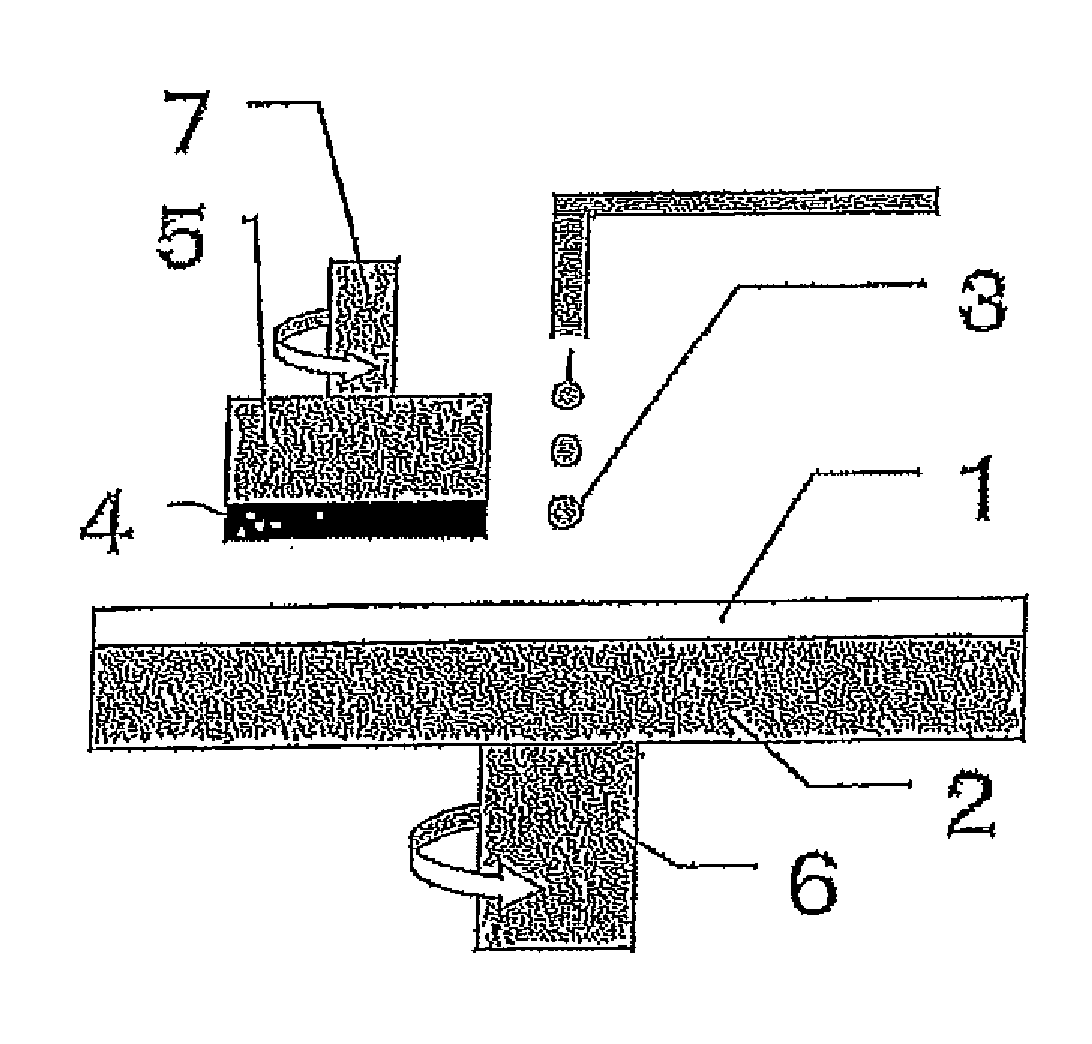
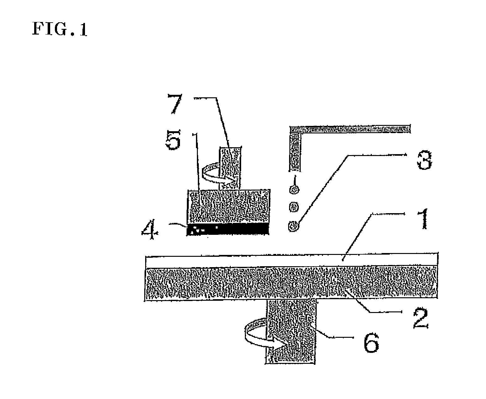
The present invention provides a polishing pad with a triple phase separation structure that has a high polishing rate and excellent planarization characteristics, while being capable of suppressing the occurrence of scratches. The method of manufacturing a semiconductor device using this polishing pad is also provided. The polishing layer is formed by using a reaction cured body with a triple phase separation structure, which has a soft phase, a crystalline phase, and a hard phase. The polishing rate is improved by surface dressing the polishing layer using a conditioner. The content of polyether polyol (D) in the prepolymer-forming raw material compositions is preferably 4 to 50% by weight based on the total weight of the high molecular weight polyol.

Problems solved by technology

In the case where such hard pads are used, however, a problem may occur in which scratches (scars) are more likely to occur on the surface of the material being polished.

Method used


Image

  • Polishing pad
  • Polishing pad
  • Polishing pad

Examples


example 1

[0105]To a vessel were added 259 parts by weight of toluene diisocyanate (a mixture of 2,4-diisocyanate / 2,6-diisocyanate=80 / 20) and 741 parts by weight of polyethylene adipate glycol with a number average molecular weight of 1,000 and allowed to react at 70° C. for 4 hours, so that an isocyanate-terminated prepolymer (A) was obtained.

[0106]To a vessel were added 392 parts by weight of toluene diisocyanate (a mixture of 2,4-diisocyanate / 2,6-diisocyanate=80 / 20), 88 parts by weight of isophorone diisocyanate, 53 parts by weight of polytetramethylene ether glycol having a number average molecular weight of 2000, 106 parts by weight of polytetramethylene ether glycol having a number average molecular weight of 1000, 103 parts by weight of polytetramethylene ether glycol having a number average molecular weight of 650, and 258 parts by weight of polytetramethylene ether glycol having a number average molecular weight of 250, and the mixture was allowed to react at 70° C. for 4 hours, so t...


PUM

PropertyMeasurementUnit
Lengthaaaaaaaaaa
Percent by massaaaaaaaaaa

Abstract

A polishing pad includes a polishing layer, and the polishing layer is formed of a reaction cured body of a polyurethane-forming raw material composition that contains: an isocyanate-terminated prepolymer (A) which is obtained by reacting a prepolymer-forming raw material composition (a) that contains an isocyanate component and a polyester polyol; an isocyanate-terminated prepolymer (B) which is obtained by reacting a prepolymer-forming raw material composition (b) that contains an isocyanate component and a polyether polyol; and a chain extender. The polyether polyol contains a polyether polyol (C) that has a number average molecular weight of 1000 or less and a polyether polyol (D) that has a number average molecular weight of 1900 or more. The reaction cured body has a triple phase separation structure.

Description

TECHNICAL FIELD[0001]The invention relates to a polishing pad capable of performing planarization of materials requiring a high surface planarity such as optical materials including a lens and a reflecting mirror, a silicon wafer, a glass substrate or an aluminum substrates for a hard disc and a product of general metal polishing with stability and a high polishing efficiency. A polishing pad of the invention is preferably employed, especially, in a planarization step of a silicon wafer or a device on which an oxide layer or a metal layer has been formed prior to further stacking an oxide layer or a metal layer thereon.BACKGROUND ART[0002]Typical materials requiring surface flatness at high level include a single-crystal silicon disk called a silicon wafer for producing semiconductor integrated circuits (IC, LSI). The surface of the silicon wafer should be flattened highly accurately in a process of producing IC, LSI etc., in order to provide reliable semiconductor connections for v...

Claims


Application Information

Patent Timeline
IPC IPC(8): B24B37/24H01L21/306C08G18/76C08G18/32C08G18/34
CPCB24B37/24C08G18/3203H01L21/30625C08G18/7621C08G18/341C08G18/10C08G18/42C08G18/48C08G18/4854C08G18/12C08G18/4238
Inventor SHIMIZU, SHINJI
Owner ROHM & HAAS ELECTRONICS MATERIALS CMP HLDG INC
Learn More