
Integrated circuits having magnetic tunnel junctions (MTJ) and methods for fabricating the same

Inactive Publication Date: 2015-11-12
GLOBALFOUNDRIES INC
View PDF5 Cites 82 Cited by
  • Summary
  • Abstract
  • Description
  • Claims
  • Application Information

AI Technical Summary

Benefits of technology

This patent describes methods and structures for fabricating integrated circuits with MTJs (which are used in magnetic memory devices) and semiconductor devices. The methods involve depositing and etching layers of materials to create the desired structures. The technical effects of the patent include improving the accuracy and efficiency of the fabrication process and creating more reliable and efficient integrated circuits.

Problems solved by technology

A critical challenge in MRAM technology is the patterning of the various layers forming the MTJ.
Conventional processing to form the MJT necessitates the use of several lithography masks and may be time-consuming.

Method used


Image

  • Integrated circuits having magnetic tunnel junctions (MTJ) and methods for fabricating the same
  • Integrated circuits having magnetic tunnel junctions (MTJ) and methods for fabricating the same
  • Integrated circuits having magnetic tunnel junctions (MTJ) and methods for fabricating the same

Examples


Embodiment Construction

[0010]The following detailed description is merely exemplary in nature and is not intended to limit the various embodiments of the integrated circuits or the methods for fabricating the integrated circuits claimed herein. Furthermore, there is no intention to be bound by any expressed or implied theory presented in the preceding technical field, background or brief summary, or in the following detailed description. Also, additional components may be included in the integrated circuits, and additional processes may be included in the fabrication methods but are not described herein for purposes of clarity. For the purposes of explanation, numerous specific details are set forth in order to provide a thorough understanding of exemplary embodiments. It should be apparent, however, that exemplary embodiments may be practiced without these specific details or with an equivalent arrangement.

[0011]Methods for fabricating integrated circuits having MTJs as described herein provide increased...


PUM


Abstract

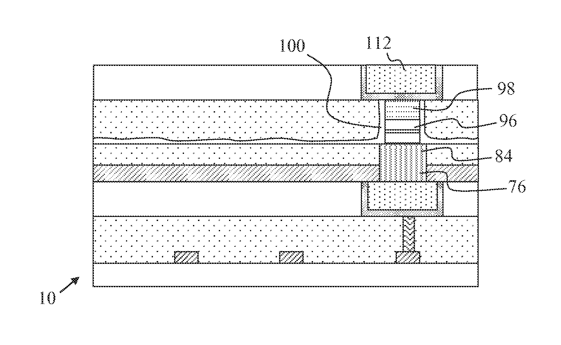
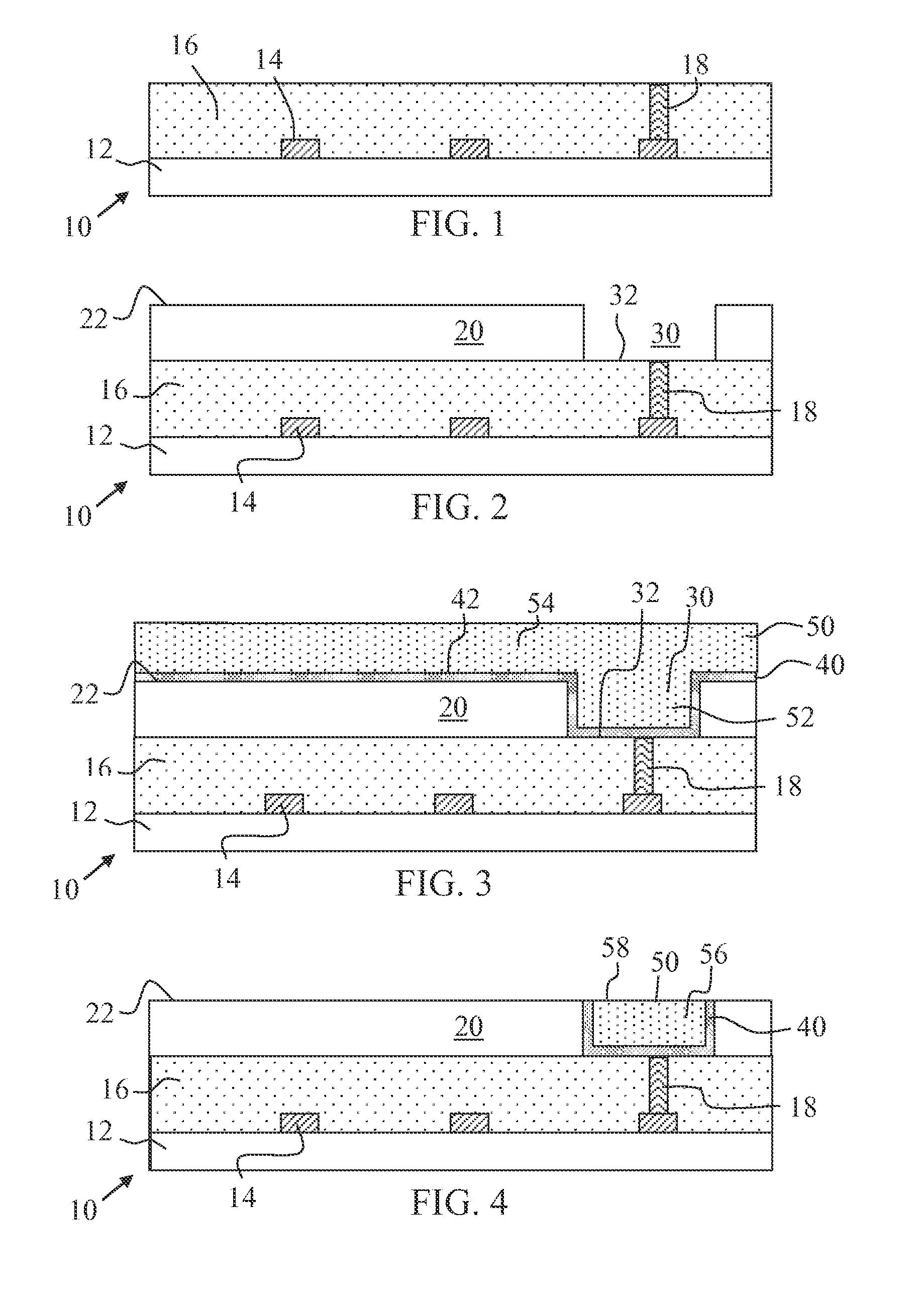
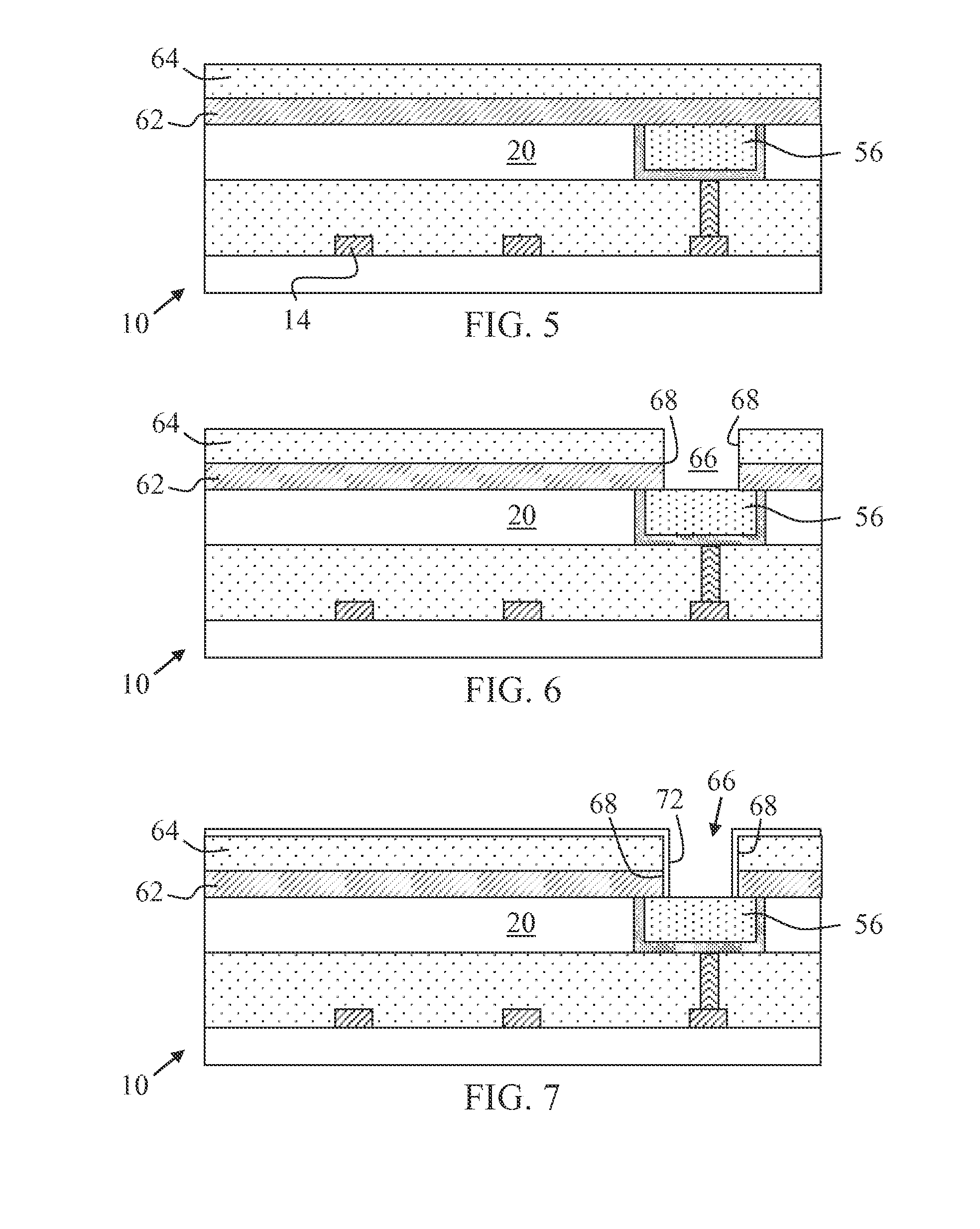
Integrated circuits with magnetic tunnel junction (MTJ) structures and methods for fabricating integrated circuits with MTJ structures are provided. An exemplary method for fabricating an integrated circuit includes forming a first conductive line in electrical connection with an underlying semiconductor device. The method exposes a surface of the first conductive line. Further, the method selectively deposits a conductive material on the surface of the first conductive line to form an electrode contact. The method includes forming a MTJ structure over the electrode contact.

Description

TECHNICAL FIELD[0001]The technical field generally relates to integrated circuits and methods for fabricating integrated circuits, and more particularly relates to integrated circuits and methods for fabricating integrated circuits having magnetic tunnel junctions (MTJs).BACKGROUND[0002]Unlike conventional random access memory (RAM) chip technologies, magnetic RAM (MRAM) does not store data as electric charge, but instead stores data by magnetic polarization of storage elements. Typically, storage elements are formed from two ferromagnetic layers separated by a tunneling layer. One of the ferromagnetic layers has at least one pinned magnetic polarization (or fixed layer) set to a particular polarity. The magnetic polarity of the other ferromagnetic layer (or free layer) is altered to represent either a “1” (i.e., anti-parallel polarity to the fixed layer) or “0” (i.e., parallel polarity to the fixed layer). One device having a fixed layer, a tunneling layer, and a free layer is a ma...

Claims


Application Information

Patent Timeline
Patent Type & Authority Applications(United States)
IPC IPC(8): H01L27/22H01L43/08H01L43/02H01L43/12
CPCH01L27/222H01L43/02H01L43/08H01L43/12H10B61/00H10N50/01H10N50/10H10N50/80
Inventor ZHANG, XUNYUANLIN, SEAN XUANTANWAR, KUNALJEET
Owner GLOBALFOUNDRIES INC
Learn More