Hydrogen-free silicon-based deposited dielectric films for NANO device fabrication

a technology of dielectric films and silicon-based deposited dielectric films, which is applied in the field of semiconductor fabrication, can solve problems such as reliability problems

Active Publication Date: 2015-10-08
IBM CORP
View PDF4 Cites 20 Cited by
  • Summary
  • Abstract
  • Description
  • Claims
  • Application Information

AI Technical Summary

Benefits of technology

The present invention provides methods for forming a dielectric film with good adhesion, low wet etched damage, low shrinkage, and high reliability. The methods involve using a hydrogen-free precursor and a plasma to create sublayers of the film. The resulting film has high purity and low defects, making it suitable for use in semiconductor devices. A semiconductor structure and semiconductor device comprising the film are also provided. The technical effects are improved reliability and performance of semiconductor devices.

Problems solved by technology

As a result, most of these dielectrics used in FEOL (front end of line) and BEOL (back end of line) silicon integrated circuit fabrication have a significant amount of weakly bonded hydrogen that can have a negative reliability impact to electronic devices, Furthermore, UV and E-Beam processing that have been recently implemented in sub-50 nm (for ULK curing or UV / E-beam lithography) devices can break the weak hydrogen bonds and release hydrogen atoms, and subsequently cause reliability issues.

Method used


Image

  • Hydrogen-free silicon-based deposited dielectric films for NANO device fabrication
  • Hydrogen-free silicon-based deposited dielectric films for NANO device fabrication
  • Hydrogen-free silicon-based deposited dielectric films for NANO device fabrication

Examples


Embodiment Construction

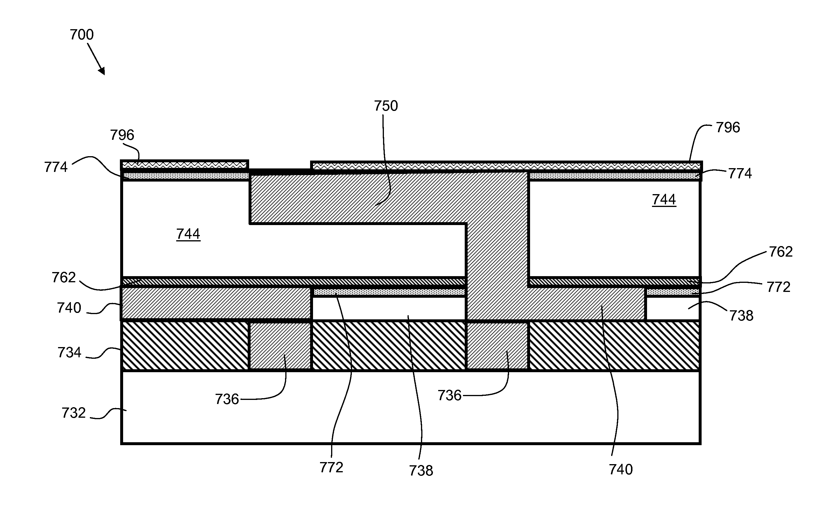
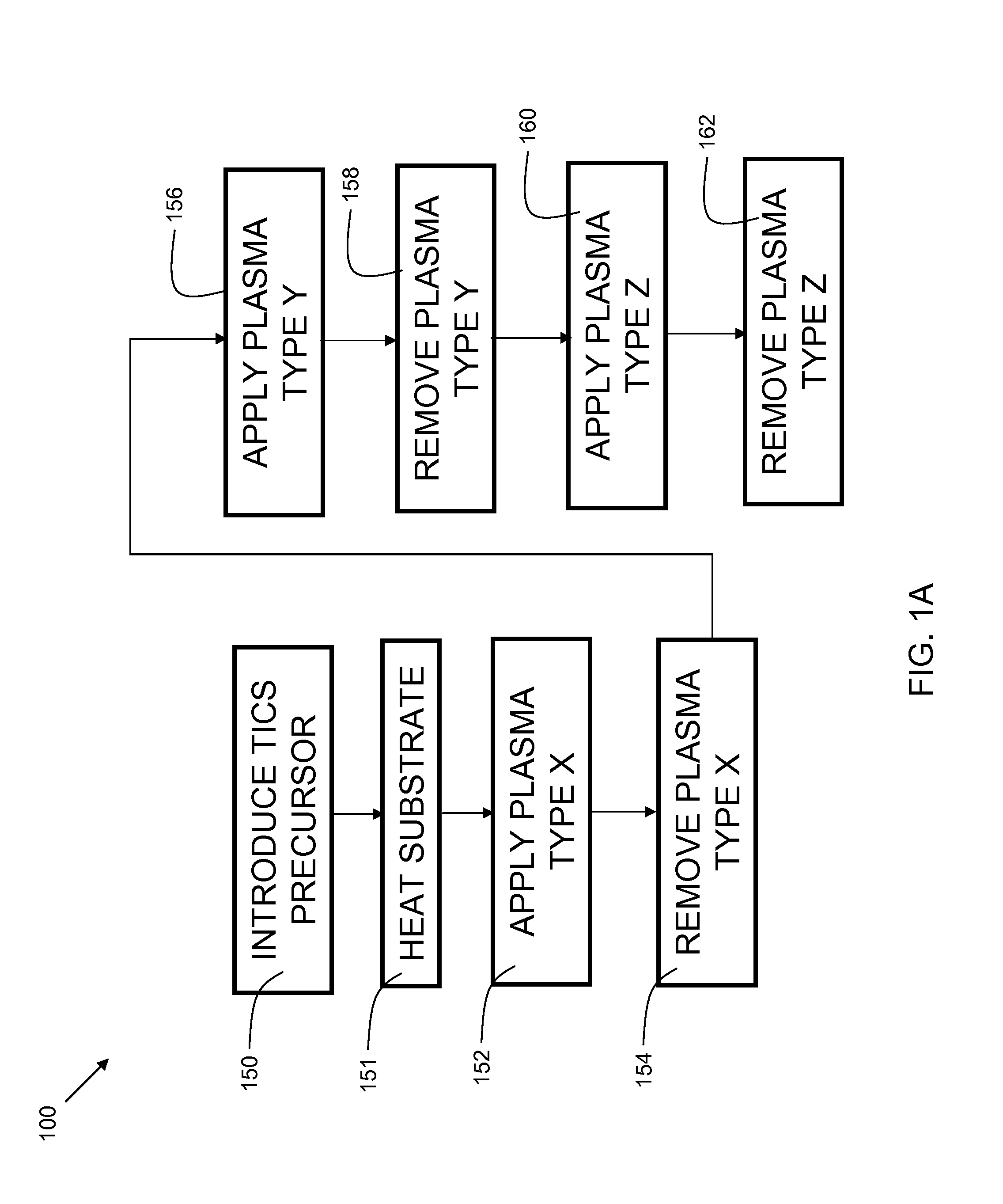
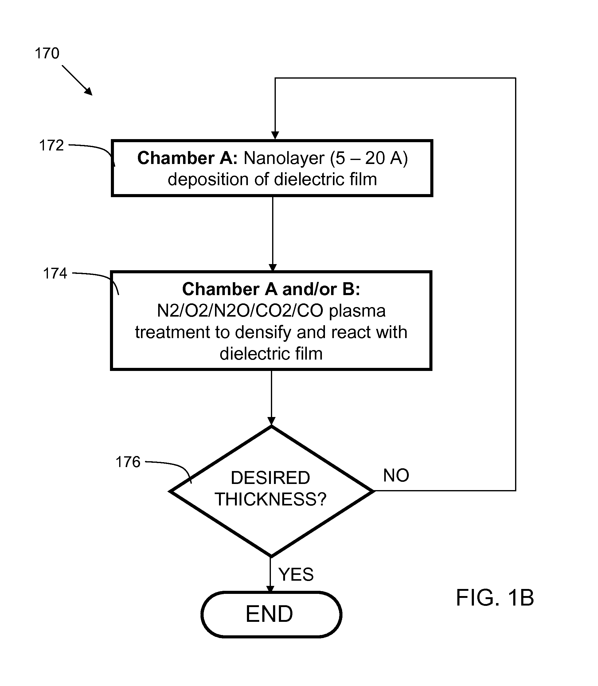
[0022]Embodiments of the present invention provide hydrogen-free dielectric films and methods of fabrication. A hydrogen-free precursor, such as tetraisocyanatosilane, and hydrogen-free reactants, such as nitrogen, oxygen (O2 / O3) and nitrous oxide are used with chemical vapor deposition processes (PECVD, thermal CVD, SACVD, HDP CVD, and PE and Thermal ALD) to create hydrogen-free dielectric films. In some embodiments, there are multilayer dielectric films with sublayers of various materials such as silicon oxide, silicon nitride, and silicon oxynitride. In embodiments, the hydrogen-free reactants may include TICS, along with a hydrogen-free gas including, but not limited to, N2, O2, O3, N2O, CO2, CO and a combination thereof of these H-Free gases. Plasma may be used to enhance the reaction between the TICS and the other H-free gasses. The plasma may be controlled during film deposition to achieve variable density within each sublayer of the films.

[0023]FIG. 1A is a flowchart 100 ind...


PUM

PropertyMeasurementUnit
Temperatureaaaaaaaaaa
Flow rateaaaaaaaaaa

Abstract

Embodiments of the present invention provide hydrogen-free dielectric films and methods of fabrication. A hydrogen-free precursor, such as tetraisocyanatosilane, and hydrogen-free reactants, such as nitrogen, oxygen (O2 / O3) and nitrous oxide are used with chemical vapor deposition processes (PECVD, thermal CVD, SACVD, HDP CVD, and PE and Thermal ALD) to create hydrogen-free dielectric films. In some embodiments, there are multilayer dielectric films with sublayers of various materials such as silicon oxide, silicon nitride, and silicon oxynitride. In embodiments, the hydrogen-free reactants may include Tetra Isocyanato Silane, along with a hydrogen-free gas including, but not limited to, N2, O2, O3, N2O, CO2, CO and a combination thereof of these H-Free gases. Plasma may be used to enhance the reaction between the TICS and the other H-free gasses. The plasma may be controlled during film deposition to achieve variable density within each sublayer of the films.

Description

FIELD OF THE INVENTION[0001]The present invention relates generally to semiconductor fabrication, and more particularly, to hydrogen-free dielectric films and methods of fabrication.BACKGROUND OF THE INVENTION[0002]For a long time, silicon-based integrated circuits (IC)s have been fabricated using a silicon dielectric such as silicon oxide. These films are heretofore formed using various hydrogen-bearing precursors. These hydrogen-bearing precursors, are mostly in gas or liquid form and are widely used due to their ease of implementation into a chemical vapor deposition (CVD) process or a plasma enhanced CVD (PECVD) process. As a result, most of these dielectrics used in FEOL (front end of line) and BEOL (back end of line) silicon integrated circuit fabrication have a significant amount of weakly bonded hydrogen that can have a negative reliability impact to electronic devices, Furthermore, UV and E-Beam processing that have been recently implemented in sub-50 nm (for ULK curing or ...

Claims


Application Information

Patent Timeline
IPC IPC(8): H01L21/02H01L29/51H01L23/532
CPCH01L21/02274H01L21/02164H01L21/0217H01L21/02126H01L21/0214H01L21/02299H01L21/02211H01L23/53295H01L29/511H01L23/485H01L23/53276H01L2924/0002H01L29/4983H01L29/513H01L29/78H01L21/76832H01L21/76834H01L21/02167H01L21/022C23C16/45523C23C16/50H01L21/02214H01L23/5329C23C16/345C23C16/401H01L2924/00H01L21/02219C23C16/45525H01L23/5226H01L23/528H01L21/02123H01L29/42364
Inventor CANAPERI, DONALD FRANCISGRILL, ALFREDMEHTA, SANJAY C.NGUYEN, SON VANPRIYADARSHINI, DEEPIKASHOBHA, HOSADURGASHOUDY, MATTHEW T.
Owner IBM CORP
Why Eureka
Try Eureka